


| Issue |
J. Eur. Opt. Society-Rapid Publ.
Volume 22, Number 2, 2026
|
|
|---|---|---|
| Article Number | 57 | |
| Number of page(s) | 10 | |
| DOI | https://doi.org/10.1051/jeos/2026048 | |
| Published online | 14 July 2026 | |
Research Article
Tungsten-rhenium alloy as a high-density absorber in ultra-short-period multilayer for hard X-ray mirrors
1
Université Paris-Saclay, Institut d’Optique Graduate School, CNRS, Laboratoire Charles Fabry, 91127, Palaiseau, France
2
CEA, Centre DAM Île-de-France, F-91197 Arpajon, France
3
CentraleSupélec, ENS Paris-Saclay, CNRS, LMPS – Laboratoire de Mécanique Paris-Saclay, Université Paris-Saclay, Gif-sur-Yvette, 91190, France
4
European Synchrotron Radiation Facility (ESRF), 71 Avenue des Martyrs, 38000 Grenoble, France
5
Physikalisch-Technische Bundesanstalt (PTB), Abbestr. 2-12, 10587 Berlin, Germany
* Corresponding author: This email address is being protected from spambots. You need JavaScript enabled to view it.
Received:
22
April
2026
Accepted:
26
May
2026
Abstract
Ultra-short-period multilayer mirrors (period d below 5 nm) are key components for hard X-ray optics in the 20 keV–40 keV range, but their performance rapidly degrades when the period approaches a few nanometers due to density loss and/or interfacial defects (roughness or intermixing). In this work, we investigate a tungsten–rhenium alloy absorber (WRe, 50 at.% Re) in WRe/SiC multilayers and compare it with a pure W absorber. We also assess the impact of the magnetron sputtering mode, conventional direct-current magnetron sputtering (dcMS) versus high-power impulse magnetron sputtering (HiPIMS), on the optical contrast and reflectivity of WRe/SiC multilayers with d ≈ 3 nm. Four periodic stacks [Abs/SiC]40 (Abs = W or WRe) were deposited and characterized by multi-energy X-ray reflectometry from a laboratory diffractometer and synchrotron beamlines (BAMline-BESSY-II and BM05–ESRF). Simultaneous fitting of reflectivity curves at multiple photon energies yields estimates of period, densities, and interfacial roughness. This specific fitting process is based on a sequential approach, providing an accurate structure model. These results are complemented by high-resolution TEM analysis of the microstructure. Compared with W/SiC, WRe/SiC exhibits a higher absorber density and a lower spacer density (SiC). This significant increase in the density contrast between the absorber and the spacer results in higher peak reflectivity at comparable Bragg angles. Under these conditions, dense WRe layers are obtained by dcMS, and HiPIMS provides similar densification within experimental uncertainties, while preserving the interfacial quality. These results demonstrate that WRe/SiC multilayers are a promising alternative to conventional W/SiC systems for high-energy X-ray mirrors at nanometer-scale periods.
Key words: Hard X-ray optics / Ultra-short-period multilayers / Tungsten–rhenium alloys / High-power impulse magnetron sputtering (HiPIMS) / Interface roughness / Intermixing
© The Author(s), published by EDP Sciences, 2026
 This is an Open Access article distributed under the terms of the Creative Commons Attribution License (https://creativecommons.org/licenses/by/4.0), which permits unrestricted use, distribution, and reproduction in any medium, provided the original work is properly cited.
1 Introduction
High-efficiency X-ray mirrors in the 20 keV to 40 keV energy range require ultra-short-period multilayer (ML) structures with periods of 1 nm–5 nm, operating at grazing angles below 1°. Such mirrors are essential for numerous applications, including hard X-ray astronomy [1], advanced lithography [2, 3], synchrotron beamlines [4], medical imaging [5], and plasma diagnostics for inertial confinement fusion experiments [6, 7].
At these high energies, ML reflectivity is primarily governed by two factors: the density difference Δρ = ρAbsorber − ρSpacer between absorber and spacer layers, and the interfacial quality (roughness and intermixing). Conventional tungsten-based multilayers, such as W/SiC, W/B4C, or W/C [8–10], can therefore suffer from reduced performance when the period is pushed to very small values and/or when the deposition conditions are not sufficiently optimized, leading to incomplete densification and increased interfacial broadening.
In a previous simulation-based study [11], we demonstrated that integrated reflectivity of the first Bragg peak Rint exhibits strong sensitivity to Δρ at high energies. Figure 1 illustrates this trend for a [W/SiC]40 multilayer in which the tungsten density is gradually varied. A modest change in the density contrast Δρ produces a pronounced variation in the integrated reflectivity Rint, whereas the peak reflectivity Rmax is comparatively less sensitive. The integrated reflectivity is therefore the most relevant figure of merit at high photon energies: although Rmax can be increased by raising the number of periods N (potentially up to several hundred, owing to the low absorption in this range), this enhancement is obtained at the expense of a reduced bandwidth and consequently a lower Rint.
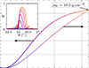 |
Figure 1 Simulated dependence of peak reflectivity |


This trade-off highlights the importance of maximizing Δρ for applications that require high performance across broad angular and spectral ranges.
Two complementary strategies can be pursued to enhance ML performance at ultra-short periods: (i) increasing the absorber density through material selection, and (ii) improving interfacial quality and film densification through advanced deposition techniques. In this work, we investigate both approaches by combining tungsten-rhenium (WRe) alloys and High-Power Impulse Magnetron Sputtering (HiPIMS) [12].
Tungsten–rhenium (WRe) alloys are a promising choice because the W50Re50 composition exhibits an amorphous phase over a wide temperature range. [13] This is beneficial for multilayer mirrors, since crystallization typically promotes strong roughness amplification and interface degradation. WRe alloys have been successfully employed as thin films in thermocouples [14], diffusion barriers [13], and corrosion protective coatings [15]. To the best of our knowledge, reports on WRe-based ultra-short-period multilayers remain sparse and are largely confined to early works from the 1980s [16–19]. Rhenium (Z = 75, bulk density ρRe = 21.02 g cm−3) [20] offers a density ∼9% higher than tungsten (ρW = 19.25 g cm−3), while remaining more cost-effective than other high-Z refractory metals such as iridium, or platinum for magnetron sputtering applications requiring high amount of materiel.
Complementary to material optimization, HiPIMS deposition generates high-energy metallic ion fluxes that enhance adatom mobility compared to conventional direct current magnetron sputtering (dcMS) [21, 22]. This increased mobility promotes void filling and interface smoothening, resulting in denser films with reduced interfacial roughness [23, 24]. The combination of higher intrinsic density (WRe) and improved densification (HiPIMS) is expected to yield significant performance gains for ultra-short-period MLs.
In this article, we report a characterization of WRe/SiC MLs with a period of d ≈ 3 nm, comparing dcMS and HiPIMS deposition methods. Using multi-energy X-ray reflectometry (XRR), and high-resolution scanning transmission electron microscopy (HR-STEM), we provide quantitative insights into the influence of both material composition and deposition technique on interfacial quality, layer density, and reflective performance in the 20 keV to 40 keV range.
2 Multilayer design and sample preparation
2.1 Optical principles
Hard X-ray multilayers consist of alternating layers of a high-density absorber and a low-density spacer. Each material is characterized by a complex refractive index  and a mass density ρ, where E is the photon energy.
The real part of the refractive index, 1 − δ(E), is directly related to the material mass density ρ through [25]: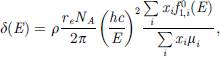 (1)where
  is the classical electron radius,
  the Avogadro constant, h the Planck constant, and c the speed of light. The term
  denotes the real part of the atomic scattering factor of element i, weighted by its atomic fraction
  , and
, and  is the atomic weight of element i. This linear dependence of δ on mass density explains why increasing the absorber density directly enhances the optical contrast
  , thereby increasing the Fresnel reflection coefficient at each interface and ultimately improving the multilayer reflectivity.
Constructive interference in a multilayer occurs when the Bragg condition is fulfilled: (2)where θ is the grazing incidence angle, d is the multilayer period, m is the Bragg order, and
  is the period-averaged real part of refractive index. The square root term accounts for refraction within the multilayer structure.
For the first Bragg order (m = 1) at a photon energy of 30 keV, Bragg’s law (Eq. (2)) yields a period of d ≈ 3 nm at a grazing angle of θ = 0.4°. The stacking ratio Γ, defined as the ratio of the absorber layer thickness to the total bilayer period d, is set to Γ ≈ 0.5 for all samples, ensuring a balanced partition between absorber and spacer thicknesses. This balanced Γ value avoids excessively thin individual layers (the absorber or the spacer below ∼1 nm), which would result in severe interface degradation and compromise multilayer performance [26].
Although B4C and C exhibit comparable low densities and favorable optical properties for hard X-ray multilayer spacers [4], SiC was selected as the spacer material based on its low bulk density (3.16 g cm−3), good chemical stability, and smooth interface formation in W-based multilayers, as well as on extensive previous in-house work [5–7, 23].
All samples include SiC buffer layers (5–10 nm thick) at the substrate of the ML and a cap layer to protect the multilayer from oxidation.
2.2 Periodic samples for X-ray reflectometry
Periodic multilayers were deposited on low-roughness silica substrates (σrms < 0.3 nm) to minimize substrate contributions to interface roughness and to have a good planarity. The structure consists of 40 bilayers of [Abs/SiC] where Abs = W or WRe, encapsulated between two SiC layers (∼8 nm), as illustrated in Figure 2a. Four samples were fabricated to explore the effects of absorber material (W vs. WRe) and deposition mode (dcMS vs. HiPIMS):
W-DC-31 and W-DC-25: W/SiC multilayers deposited by dcMS, with different targeted periods to assess repeatability and period-dependent trends.
WRe-DC-46: WRe/SiC multilayer deposited by dcMS, to quantify the effect of substituting W with WRe on density and interface quality.
WRe-HP-26: WRe/SiC multilayer deposited by HiPIMS, combining the benefits of higher intrinsic density (WRe) and enhanced densification (HiPIMS).
 |
Figure 2 Schematic structures of samples prepared for (a) X-ray reflectometry and (b) transmission electron microscopy (TEM) measurements. |
Deposition parameters and structural characteristics extracted from multi-energy XRR fitting (see Sect. 3.1.1) are summarized in Table 1.
Deposition parameters and fitted structural properties of periodic multilayers for XRR. Uncertainties on fitted values are obtained from the sensitivity analysis of XRR fits at multiple energies.
2.3 Aperiodic samples for transmission electron microscopy
Aperiodic multilayers for TEM were deposited on Si(100) wafers (σrms < 0.25 nm). Each sample consists of two distinct stacks deposited on the same substrate (Fig. 2b), enabling direct comparison between materials or deposition modes under identical TEM preparation and imaging conditions, thereby eliminating systematic uncertainties related to lamella preparation, sample alignment, or microscope settings. Each stack comprises seven subgroups of N bilayers with periods ranging from 1.5 nm to 6 nm, as detailed in Table 2. This aperiodic design allows simultaneous characterization of interface quality across a range of period thicknesses within a single cross-sectional TEM lamella, providing insights into the period-dependent evolution of interface morphology that cannot be obtained from periodic samples alone.
Targeted aperiodic structure for TEM samples. Each subgroup consists of N bilayers with period d and stacking ratio Γ ≈ 0.5. Subgroups are stacked vertically from substrate (subgroup 7, thinnest period) to surface (subgroup 1, largest period).
Two TEM samples were fabricated to isolate the effects of material composition and deposition mode:
TEM-73: stack 1 is W/SiC (dcMS) and stack 2 is WRe/SiC (dcMS), to assess the influence of absorber composition on interface morphology while keeping the deposition process constant.
TEM-65: stack 1 is WRe/SiC (dcMS) and stack 2 WRe/SiC (HiPIMS), to assess the influence of deposition mode on interface quality while keeping the material composition constant.
2.4 Deposition system and conditions
All samples were deposited using a Plassys MP1000SL magnetron sputtering system at Laboratoire Charles Fabry. The chamber is equipped with four rectangular targets (200 mm × 80 mm) distributed around the chamber on a circular geometry. The substrates are mounted on a rotating platter (substrate holder), so that during deposition, each sample passes sequentially above a target. Each magnetron has a confinement box that locally encloses the plasma above the target.
Tungsten (W) and tungsten–rhenium (WRe at 50–50 at.% Re) absorber layers were deposited using either dcMS or HiPIMS, while silicon carbide (SiC) spacer layers were deposited by radio-frequency magnetron sputtering (rfMS) in all cases. All targets have purity >99.9%. For the HiPIMS power supply, we use an HIPSTER-1 from Ionautics.
Depositions were performed at room temperature using argon as the sputtering gas. The base pressure was 5 × 10⁻⁸ Torr, and the working pressure was maintained at 2 mTorr with an Ar flow rate of 50 sccm. The target-to-substrate distance was 80 mm. Trapezoidal masks positioned between targets and substrate compensate for non-uniform sputtering flux distribution, ensuring lateral thickness uniformity across the deposition area.
2.5 Simulation methods
Specular X-ray reflectivity curves are computed using the recursive Parratt formalism [27], implemented in a custom Python script. Optical constants ( ,
,  ) are obtained from the Henke database [28] for photon energies below 30 keV and from NIST-CHANTLER tables [29] at higher energies. Interfacial roughness is modeled using the Névot-Croce formalism [30], which accounts for a Gaussian distribution of interface height fluctuations with root-mean-square roughness σ.
3 Experimental results
3.1 X-ray reflectometry
3.1.1 Experimental setup
Specular X-ray reflectivity measurements were performed at multiple photon energies to enable robust structural characterization by simultaneously fitting multi-energy data sets.
In-house measurements were carried out using a Bruker D8 diffractometer equipped with a Cu tube source equipped with a Göbel mirror to select Kα lines (E = 8.048 keV, λ = 0.154 nm) in θ-2θ geometry. These measurements provide high angular resolution over a wide angular range, enabling accurate determination of the multilayer period from Bragg peak positions, overall structural coherence from Kiessig fringes, and initial estimates of interfacial roughness. Measurements at 8.048 keV are presented in Figure 3 for all four samples with the final fitted curves (see Sect. 3.1.2).
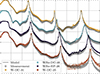 |
Figure 3 Reflectivity curve of all sample measures at 8.048 keV with fitted curve in solid lines. |
High-energy reflectivity measurements were conducted at two synchrotron facilities to probe the first Bragg peak under conditions relevant for practical applications (20 keV to 40 keV):
BAMline at BESSY-II [31]: Measurements at photon energy from 20 keV to 30 keV were performed using a photodiode detector with a 300 μm entrance slit ensuring adequate angular resolution while maintaining sufficient flux.
BM05 at ESRF [32]: Measurements were performed in the 20 keV to 60 keV energy range, corresponding to the beamline’s maximum flux region. The acquisition setup consists of an Andor Marana 11 sCMOS camera coupled to a 9 × 9 mm2 Ce:YAG scintillator via a 2× magnification objective. Each data point corresponds to an image acquired at multiple exposure times (from 0.01 s to 1 s), providing a high dynamic range while maintaining a relatively fast acquisition rate. This two-dimensional detector enables the selection of a region of interest after measurement.
The use of two independent beamlines with different detector technologies provides cross-validation of the measured reflectivity curves and eliminates potential systematic errors associated with a single experimental configuration.
3.1.2 Data analysis and fitting procedure
Reflectivity curves acquired at multiple energies (8 keV, 20 keV, 30 keV, and 40 keV) were fitted simultaneously using a single structural model to ensure self-consistency. In practice, we found that a direct approach (i.e., allowing all parameters to vary simultaneously from generic initial guesses) often fails to converge toward physically realistic solutions, due to strong parameter correlations at ultra-short periods (notably between Γ, layer densities, and interfacial roughness), and the presence of multiple local minima yielding comparably good agreement at a single energy. After testing several fitting strategies (including global refinements with randomized initial conditions), we identified a sequential procedure that provides more stable convergence and consistently yields physically meaningful parameters. While this approach is inherently more guided and, therefore, potentially more biased, it explicitly incorporates our prior knowledge of how each parameter affects distinct features of the reflectivity curves. The fits, illustrated in Figure 4, follow the sequential approach outlined below:
The multilayer period d is initially determined from the angular position of Bragg peaks in the 8 keV data.
The Γ ratio is adjusted to reproduce the overall reflectivity curve shape, relative peak intensities, and peak extinction (since
 , the even orders are strongly suppressed).
Interfacial roughness parameters (σabs/SiC and σSiC/abs) are optimized using a genetic algorithm to match the decay of Bragg peak intensities with increasing order and the amplitude of Kiessig fringes.
Material densities (ρabs and ρSiC) are refined to simultaneously match: (i) the critical angle position, which depends on the period-averaged density
 , and (ii) the peak reflectivity magnitude, which depends on the density contrast Δρ = ρabs − ρSiC.
The fitted model is tested against high-energy synchrotron data (20 keV to 40 keV). Steps 3 and 4 are iterated until convergence.
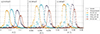 |
Figure 4 X-ray reflectivity measurements (symbols) and corresponding best-fit simulations (solid lines) for the four periodic multilayer samples at three photon energies: (a) 8 keV (Cu Kα, Bruker D8), (b) 30 keV (W-DC-31 and W-DC-25 data from PTB-BAMline, others from ESRF-BM05), and (c) 40 keV (all from ESRF-BM05). |
This multi-energy fitting approach strongly constrains the structural parameters, yielding more reliable estimates of layer densities and interface quality than single-energy analysis. Figure 4 demonstrates the good agreement between experimental reflectivity data and the fitted model across all photon energies (8 keV, 30 keV, and 40 keV) for all four samples, using the parameters listed in Table 1. The ability of a single structural model to reproduce the reflectivity curves at multiple energies validates the robustness and self-consistency of the estimated parameters.
We incorporated an angular-resolution parameter into the simulated curves to account for each instrument’s angular resolution, as this can significantly influence the reflectivity curve [33]. We also introduced a relative d-spacing error to account for deposition-induced period variations during growth. This parameter broadens the high-order Bragg peaks and remains below 1% for all samples.
Across the full dataset, the reflectivity curves acquired at different energies are well aligned, with the remaining small angular offsets staying below the alignment precision of the measurement setup. This further supports the benefit of the multi-energy approach, which averages out such minor experimental shifts and yields the most representative, self-consistent reflectivity dataset.
3.2 Scanning transmission electron microscopy
3.2.1 Experimental setup
Cross-sectional lamellae for transmission electron microscopy were prepared by focused-ion-beam (FIB) milling in a scanning electron microscope (SEM) using a FEI ThermoFisher Helios Nanolab 660. High-resolution high-angle annular dark-field scanning transmission electron microscopy (HR-HAADF-STEM) imaging was performed using an FEI Titan G2 80–300 microscope operated at 300 at the Laboratoire de Mécanique Paris-Saclay.
The HAADF-STEM imaging mode exploits Z-contrast, where Z is the atomic number. This produces bright intensity from high-Z absorber layers (W: Z=74, Re: Z=75) and dark intensity from low-Z spacer layers (Si: Z=14, C: Z=6), providing excellent discrimination between materials with minimal diffraction contrast artifacts.
3.2.2 Quantitative analysis of TEM images
Individual layer thicknesses and interface profiles were quantified from intensity line profiles extracted perpendicular to the multilayer stack, as illustrated in Figure 5. We optimized image rotation to ensure that multilayer interfaces are aligned with the pixel grid, minimizing bias in the extracted profiles. To improve the signal-to-noise ratio, intensity profiles were averaged laterally over regions of ∼10 nm width along the y-axis, corresponding to the vertical direction in the bottom panels of Figure 5b,c.
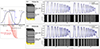 |
Figure 5 (a) Schematic illustration of the quantitative analysis procedure for HAADF-STEM images. Interface positions are determined by fitting the profile with the error function at each interface. (b) HAADF-STEM image and intensity profile for sample TEM-73, comparing WRe/SiC (top stack) and W/SiC (bottom stack), both deposited by dcMS. (c) HAADF-STEM image and intensity profile for sample TEM-65, comparing WRe/SiC deposited by dcMS (top) and HiPIMS (bottom). Brighter layers correspond to absorbers (W or WRe), darker layers to SiC spacers. |
The intensity profile I(z) was first normalized to the [0, 1] range to enable consistent analysis across different imaging conditions. For each interface indexed by i, the precise interface position zii and the transition width  were determined by fitting the normalized intensity profile in the region between consecutive local extrema (absorber and spacer peak positions) with an error function (Erf) (consistent with the error-function interface profile implied by the Névot–Croce roughness model [30]), as shown schematically in Figure 5a:
![Mathematical equation: $$ \text{Erf}_i(z) = \frac{1}{\widetilde{\sigma}_i \sqrt{2\pi}} \int_{-\infty}^{z} \exp \left[ -\frac{(z' - z_i)^2}{2\widetilde{\sigma}_i^2} \right] \text{d}z' $$](/articles/jeos/full_html/2026/02/jeos20260043/jeos20260043-eq50.gif) (3)
(3)
where zi is the center position of ith interface and  characterizes the interface transition width. A small value translates to a sharper interface. The fitted parameter
  reflects the interfacial roughness, chemical intermixing, and instrumental broadening effects. Layer thicknesses ei were calculated as the distance between successive interface centers:
  and the local period being
  .
.
Despite using the same error function to describe the interface, it is important to note that  determined from TEM is not directly equivalent to the interfacial roughness parameter σ used in the Névot-Croce model for X-ray reflectometry, due to differences in the measurement process and sensitivity to different spatial frequency ranges. Therefore, TEM-derived interface widths provide complementary rather than directly comparable information to XRR-derived roughness values.
4 Discussion
4.1 Multi-energy reflectometry analysis and period-dependent performance
To assess the impact of period thickness, absorber composition, and deposition mode on multilayer performance, we analyze the X-ray reflectivity measurements across the 8 keV to 40 keV energy range. Figure 6 shows reflectivity curves measured at various photon energies for the four samples, in solid dotted line.
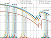 |
Figure 6 X-ray reflectivity curves measured (symbols), along with best-fit simulations (thin solid lines). The fitted structural parameters extracted from simultaneous fitting of multi-energy data are listed in Table 1. Bragg peaks and Kiessig fringes are clearly visible, indicating high structural quality. Thick solid lines are described in Section 4.1. |
A direct comparison between samples with different periods requires careful consideration, as both the Bragg angle and the achievable peak reflectivity depend on the period thickness. We propose a meaningful comparison across energies and samples with a representation plotting the peak reflectivity  as a function of its corresponding Bragg angle
  for the first-order peak. Those values are extrapolated from the multilayer model derived from all the measured data. This approach is illustrated in Figure 6 with thick solid lines. From the structural model of each sample, we extract
  by simulating angular reflectivity scans at varying photon energies, yielding a trajectory in the
  space that characterizes each sample’s performance independently of the specific measurement energy. We can observe features corresponding to the L-absorption edges of tungsten and rhenium around 1° on those computed curves. The thick solid lines in Figure 6 further validate the fitting procedure described in Section 3.1.2, demonstrating that a single structural model consistently reproduces the reflectivity at the different photon energies.
4.2 Effect of period thickness on W/SiC ML
The two W/SiC samples deposited by dcMS exhibit significantly different performance. Sample W-DC-31, with the larger period ( ), achieves peak reflectivities approaching 85% at 40 keV. In contrast, sample W-DC-25, with a shorter period (
 ), shows significantly degraded performance with
  of 64%.
This deterioration is primarily attributed to increased interfacial intermixing and roughness at reduced period thickness, as confirmed by the fitted roughness values in Table 1:  for W-DC-31 versus
  for W-DC-25. At short periods, the transition zones become comparable to individual layer thicknesses [34], meaning that interfacial defects occupy an increasingly large fraction of the total structure volume. This phenomenon leads to a drastic reduction in optical contrast (electronic density) between the absorber and spacer, thereby limiting the maximum achievable reflectivity [35, 36]. This trend is consistent with previous observations in W/B4C systems [37].
4.3 Enhanced performance with tungsten-rhenium absorbers
Despite having lower period thicknesses (d = 3.34 nm for WRe-HP-26 and d = 3.50 nm for WRe-DC-46), both WRe/SiC samples outperform (or at least equal) the performance of the longer-period W/SiC sample (W-DC-31). This enhancement is clear in Figure 6, where the WRe/SiC samples exhibit higher peak reflectivities at comparable Bragg angles. The improved performance is primarily attributed to the increased density contrast  between absorber and spacer layers. As shown in Table 1, the fitted absorber densities for WRe samples (ρWRe ≈ 16.7 g cm−3 for dcMS, 17.1 g cm−3 for HiPIMS) exceed those of W samples (ρW ≈ 15.2 g cm−3), resulting in a ∼ 10–15% increase in Δρ.
This density enhancement is further corroborated by calibration multilayer samples (with a reduced number of periods N) deposited prior to the main samples: XRR fits consistently show a shift in critical angle and higher fitted densities for WRe layers compared to pure W, confirming that the density contrast observed in the periodic multilayers is a robust and reproducible feature of the WRe absorber.
In addition, the fitted SiC spacer density (Table 1) is systematically lower for WRe/SiC samples (ρSiC ≈ 3.3 g cm−3) compared to W/SiC samples (ρSiC ≈ 4.3 g cm−3), despite identical rfMS deposition conditions for all spacer layers. This result enhances the density contrast Δρ in WRe/SiC multilayers, thereby improving their performance. The observed variation in apparent SiC density can have several origins. In W/SiC samples, the elevated fitted density (ρSiC > 3.2 g cm−3, the bulk value) likely indicates significant intermixing or interdiffusion of tungsten into the SiC layers, effectively increasing the average atomic mass within the spacer regions. Conversely, the lower fitted density in WRe/SiC samples suggests either reduced intermixing with the WRe absorber or different SiC growth dynamics on WRe versus W surfaces.
The reduced intermixing with WRe is likely thermodynamically driven. The interfacial energy balance between absorber, spacer, and their interface (γabs, γSiC, γi) determines both the growth mode and interdiffusion tendency. WRe may exhibit a higher interfacial energy or a lower chemical affinity for SiC than pure W, thereby reducing the thermodynamic driving force for intermixing despite its heavier atomic mass. Additionally, the WRe surface may provide different nucleation conditions for SiC growth, influencing the spacer microstructure (density, void content) and resulting in denser, less contaminated layers.
The fitted roughness values for WRe/SiC samples (σ ≈ 0.27 nm for dcMS, 0.31 for HiPIMS) are slightly higher than those of the thicker W/SiC sample (W-DC-31: σ ≈ 0.21 nm), but comparable to or lower than those of the thinner W/SiC sample (W-DC-25: σ ≈ 0.36 nm) despite having intermediate periods. This indicates that the better performance of WRe/SiC ML is not primarily attributable to reduced interfacial roughness, but rather to the enhanced density contrast Δρ, which increases by ∼10–15% compared to W/SiC systems (Table 1). This highlights the main role of optical contrast at these ultra-short periods, consistent with the scaling predictions of Figure 1.
By analyzing the TEM images of the sample TEM-73 via the Figure 7a we can confirm that the interface widths  of WRe/SiC are less abrupt than W/SiC, which is consistent with the fitted roughness values from XRR.
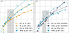 |
Figure 7 Two-by-two comparison of the MET sample groups: (a) W/SiC (dcMS) vs. WRe/SiC (dcMS) and (b) WRe/SiC (dcMS) vs. WRe/SiC (HiPIMS). The fitted interface widths |

In Figure 7, the extracted  values appear to decrease as the period d is reduced. This trend, however, is not consistent with the XRR fits reported in Table 1, which instead indicate a slight increase of the interfacial widths for the W/SiC samples (from ∼0.2 nm up to ∼0.35 nm) as d decreases from 3.65 nm to 3.28 nm. Such interfacial broadening at shorter periods is also commonly reported in the literature [26]. This discrepancy arises from the data analysis procedure. In particular, the error-function fitting approach cannot return interface widths
  larger than the local period d, which biases the extracted trend in the thinnest-period range. Nevertheless, the purpose of this analysis is primarily comparative, i.e., to assess relative differences between deposition conditions, rather than to derive absolute roughness values.
Regardless of the underlying mechanisms, the net effect is beneficial: the combination of higher absorber density and lower apparent spacer density in WRe/SiC systems maximizes Δρ, directly enhancing reflectivity.
4.4 Impact of HiPIMS
The comparison between HiPIMS and dcMS deposition modes for WRe/SiC MLs reveals a moderate impact of HiPIMS, which differs from our previous observations on W/SiC systems [23]. Samples WRe-HP-26 (HiPIMS, d = 3.34 nm) and WRe-DC-46 (dcMS, d = 3.50 keV) exhibit comparable reflectivities across the 30 keV to 40 keV range (Fig. 6), with dcMS yielding marginally higher peak values, certainly due to a higher period.
The fitted structural parameters (Table 1) do not evidence any clear HiPIMS-induced densification within the density uncertainties: ( g cm−3 vs.
  g cm−3, ∼2% gain) compared to the 10–15% improvements observed in pure W films.
TEM-derived interface widths  (Fig. 7b) show comparable values for WRe/SiC multilayers deposited by dcMS and HiPIMS, suggesting that the HiPIMS peak current of 14 A is not sufficient to significantly affect the microstructure.
However, the XRR-fitted roughness values for the WRe/SiC interface differ only slightly between HiPIMS ( = 0.35 nm) and dcMS (
 = 0.30 nm). This Δσ ≈ 0.05 nm remains on the order of our experimental repeatability and process-to-process variability, and it is further difficult to interpret unambiguously because the two samples have slightly different periods (dHiPIMS = 3.34 nm vs. ddcMS = 3.50 nm). As a result, with our HiPIMS parameters, no statistically significant HiPIMS effect on interfacial roughness can be concluded from the present dataset.
These results point to a material-dependent response to HiPIMS processing. In particular, because pure Re is significantly less electrically conductive than W [20], the electrical conductivity of WRe alloys is also reduced, which is expected to modify the discharge characteristics in HiPIMS (plasma impedance, current waveform, and ion-to-neutral ratio) compared with pure W targets. Under our conditions, this altered discharge behavior may limit the potential densification benefits of HiPIMS and/or increase ion-induced interface degradation. Further optimization of HiPIMS parameters (pulse energy, duty cycle) specifically for WRe targets is therefore likely required.
Nevertheless, both WRe/SiC samples outperform conventional W/SiC ML at comparable periods, confirming that absorber density remains a primary determinant of reflectivity in the 20 keV to 40 keV range.
5 Conclusion
We investigated tungsten–rhenium alloy absorbers (WRe, 50 at.% Re) as a way to improve the performance of ultra-short-period multilayer mirrors for hard X-rays. Periodic [Abs/SiC]40 stacks (Abs = W or WRe) were characterized by multi-energy X-ray reflectometry (8 keV to 40 keV) measurements, and interface morphology was further assessed by HR-HAADF-STEM on dedicated aperiodic samples.
Multi-energy simultaneous fitting provides self-consistent structural parameters and confirms the strong period-dependence of W/SiC performance: reducing the period from  to
to  leads to a significant reflectivity loss, consistent with the higher fitted values of interfacial intermixing/roughness. In contrast, WRe/SiC multilayers achieve peak reflectivity equal to or higher than that of W/SiC, primarily due to higher absorber density and therefore a higher density contrast. The fitted roughness values for WRe/SiC remain within a reasonable range and degrade performance (from ≈0.2 nm (W) to ≈0.3 nm (WRe)), indicating that optical contrast is a critical factor at these periods.
Finally, within the HiPIMS parameter set investigated here (peak current 14 A, 30 μs pulses at 1 kHz), no clear densification of WRe beyond the dcMS case can be resolved within the experimental uncertainties, and any change in interface widths remains smaller than our measurement and process repeatability. This suggests that WRe already reaches near the highest achievable densification in this range of period with dcMS in our configuration, and that further HiPIMS study with extended parameter values (peak current, pulse duration, bias, and ion-to-neutral ratio) will be necessary to achieve further optimization.
Although rhenium is scarcer than tungsten, its use in multilayer mirrors involves only sub-milligram quantities per device, making the raw material cost negligible at the device fabrication level. Moreover, rhenium remains significantly less expensive than other high-Z absorber candidates such as iridium or platinum [20], whose market prices exceed that of rhenium by one to two orders of magnitude [38]. Overall, WRe/SiC emerges as a robust, high-performing alternative to W/SiC for nanometer-period multilayer mirrors in the hard X-ray range, and appears to be a promising route to unlock reliable ultra-short-period coatings by alleviating the key performance limitations of conventional W-based stacks.
Funding
This work was supported by CEA-DAM.
Conflicts of interest
The authors declare no conflicts of interest.
Data availability statement
The data underlying the results presented in this paper are not publicly available at this time but may be obtained from the authors upon reasonable request.
Author contribution statement
Conceptualization, A.L. and F.D.; Methodology, C.N.; Software, C.N.; Validation, A.L. and F.D.; Formal Analysis, C.N.; Investigation, C.N., A.L. and F.D.; Resources, E.M., TN.TC., C.G., and M.V.; Data Curation, F.D. and F.D.; Writing – Original Draft Preparation, C.N.; Writing – Review & Editing, F.D. and A.L.; Supervision, F.D. and A.L.; Project Administration, F.D. and A.L.; Funding Acquisition, F.D. and A.L.
Acknowledgments
This work was performed under the auspices of the Institut d’Optique Graduate School, Université Paris-Saclay, and CEA-DAM. The authors would like to thank Louis Cornet (CentraleSupélec, Université Paris-Saclay, France) for the FIB preparation and the beamline teams from BM05-ESRF and BAMline, BESSY-II.
References
- Windt DL. Advancements in Hard X-Ray Multilayers for x-Ray Astronomy. SPIE Optical Engineering + Applications, edited by O’Dell SL et al. (San Diego, California, United States, 2015), 96031C. https://doi.org/10.1117/12.2187481. [Google Scholar]
- Tallents G et al., Lithography at EUV wavelengths. Nat. Photonics 4(12), 809–811 (2010). https://doi.org/10.1038/nphoton.2010.277. [Google Scholar]
- Kazazis D et al., Extreme ultraviolet lithography. Nat. Rev. Methods Primers 4(1), 84 (2024https://doi.org/10.1038/s43586-024-00361-z. [Google Scholar]
- Singhapong W et al., Multilayer optics for synchrotron applications. Adv. Mater. Technol. 9(18), 2302187 (2024). https://doi.org/https://doi.org/10.1002/admt.202302187. [Google Scholar]
- Windt DL. Monochromatic mammography using scanning multilayer X-ray mirrors. en (). [Google Scholar]
- Ravinet N et al., Design and simulation of multilayer coatings for a multi-channel Wolter-like x-ray imager with large field of view and high resolution. Rev. Sci. Instrum. 94(10), 103502 (2023). https://doi.org/10.1063/5.0165414. [Google Scholar]
- Ravinet N et al., Multilayer coatings for a multi channel Wolter-like x-ray imager with large field of view and high resolution: Experimental development and study of the instrument performance. Rev. Sci. Instrum. 97(4), 041304 (2026). https://doi.org/10.1063/5.0316988. [Google Scholar]
- Windt DL et al., W/SiC x-ray multilayers optimized for use above 100 keV. Appl. Opt. 42(13), 2415–2421 (2003). https://doi.org/10.1364/AO.42.002415. [Google Scholar]
- Pradhan PC et al., Fabrication and Performance of a High Resolution Ultra-Short Period W/B4 C Multilayer Structure. J. Phys. D. Appl. Phys. 49(13), 135305 (2016). https://doi.org/10.1088/0022-3727/49/13/135305. [Google Scholar]
- Chon K et al., Monochromatic X-ray imaging system using a W/C multilayer mirror. J. Korean Phys. Soc. 55(6), 2571–2577 (2009). https://doi.org/10.3938/jkps.55.2571. [Google Scholar]
- Nannini C et al., Selecting Materials for Short-Period Multilayer X-ray mirrors: Comparison between peak and integrated reflectivity. Advances in Optical Thin Films VIII, edited by Lequime M et al. Strasbourg, France: (SPIE, 2024), 67. https://doi.org/10.1117/12.3016698. [Google Scholar]
- Kouznetsov V et al., A novel pulsed magnetron sputter technique utilizing very high target power densities. Surf. Coat. Technol. 122(2), 290–293 (1999). https://doi.org/10.1016/S0257-8972(99)00292-3. [Google Scholar]
- Hörnström SE et al., Tungsten–rhenium alloys as diffusion barriers between aluminum and silicon. J. Vac. Sci. Technol. A 6(3), 1650–1655 (1988). https://doi.org/10.1116/1.575302. [Google Scholar]
- Tian B et al., Effect of magnetron sputtering parameters on adhesion properties of tungsten–rhenium thin film thermocouples. Ceram. Int. 44, S15–S18 (2018). https://doi.org/10.1016/j.ceramint.2018.08.334. [Google Scholar]
- Shapagina NA et al., Coatings based on refractory materials for corrosion and wear applications. Materials 17(23), 5936 (2024). https://doi.org/10.3390/ma17235936. [Google Scholar]
- Lee P et al., Soft X-ray optics using multilayer mirrors. Opt. Eng. 24(1), 241197 (1985). https://doi.org/10.1117/12.7973449. [Google Scholar]
- Chauvineau JP et al., The fabrication of multilayers for soft X-rays and extreme ultra-violet mirrors. J. Opt. 15(4B), 265–269 (1984). https://doi.org/10.1088/0150-536X/15/4B/306. [Google Scholar]
- Bruijn M et al., Optimization of multilayer soft Xray mirrors. Nucl. Instrum. Methods Phys. Res. 219(3), 603–606 (1984). https://doi.org/10.1016/0167-5087(84)90238-2. [Google Scholar]
- Ziegler E et al., Stability of multilayers for synchrotron optics. Appl. Phys. Lett. 48(20), 1354–1356 (1986). https://doi.org/10.1063/1.96907. [Google Scholar]
- Rumble JR, ed. CRC Handbook of Chemistry and Physics, 102 edn 2021–2022. (Boca Raton London New York: CRC Press, 2021. [Google Scholar]
- Lundin D et al., An introduction to thin film processing using high-power impulse magnetron sputtering. J. Mater. Res. 27(5), 780–792 (2012). https://doi.org/10.1557/jmr.2012.8. [Google Scholar]
- Anders A. High power impulse magnetron sputtering: A possible route to coatings for superconducting RF cavities (2010). [Google Scholar]
- Nannini C et al., HiPIMS deposition method unlocks higher X-ray reflectance in ultra-short-period multilayer mirrors. Opt. Lett. 50(21), 6513–6516 (2025). https://doi.org/10.1364/OL.571400. [Google Scholar]
- Samuelsson M et al., On the film density using high power impulse magnetron sputtering. Surf. Coat. Technol. 205(2), 591–596 (2010). https://doi.org/10.1016/j.surfcoat.2010.07.041. [Google Scholar]
- Attwood D et al., X-Rays and Extreme Ultraviolet Radiation: Principles and Applications, 2nd edn. (Cambridge: Cambridge University Press, 2017). https://doi.org/10.1017/CBO9781107477629. [Google Scholar]
- Walton C et al., X-ray optical multilayers: microstructure limits on reflectivity at ultra-short periods. Acta Mater. 46(11), 3767–3775 (1998). https://doi.org/10.1016/S1359-6454(98)00083-4. [Google Scholar]
- Parratt LG. Surface studies of solids by total reflection of X-rays. Phys. Rev. 95(2), 359–369 (1954). https://doi.org/10.1103/PhysRev.95.359. [CrossRef] [Google Scholar]
- Henke BL et al., X-ray interactions: photoabsorption, scattering, transmission, and reflection at E = 50-30,000 eV, Z = 1-92. At. Data Nucl. Data Tables 54(2), 181–342 (1993). https://doi.org/10.1006/adnd.1993.1013. [Google Scholar]
- Chantler C et al., X-Ray form factor, attenuation and scattering tables (Version 2.0). (2003). [Google Scholar]
- Névot L et al., Caractérisation des surfaces parréflexion rasante de rayons X. Application à l’étudedu polissage de quelques verres silicates. Revue de Physique Appliquée 15(3), 761–779 (1980). https://doi.org/10.1051/rphysap:01980001503076100. [Google Scholar]
- Görner W et al., BAMline: The first hard X-ray beamline at BESSY II. Nucl. Instrum. Methods Phys. Res. Sect A: Accel., Spectrometers, Detectors Associated Equip. 467–468(10), 703–706 (2001). https://doi.org/10.1016/S0168-9002(01)00466-1. [Google Scholar]
- Ziegler E. The ESRF BM05 Metrology Beamline: Instrumentation And Performance Upgrade. AIP Conference Proceedings. Vol. 705. (San Francisco, California (USA): AIP, 2004), pp. 436–439. https://doi.org/10.1063/1.1757827. [Google Scholar]
- Delmotte F et al., At wavelength metrology of high-reflectance multilayer mirror in the water window. J. Appl. Phys. 139(1), 013107 (2026). https://doi.org/10.1063/5.0310891. [Google Scholar]
- IJpes D et al., High reflectance ultrashort period W/B4C x-ray multilayers via intermittent ion polishing. J. Appl. Phys. 136(24), 245302 (2024). https://doi.org/10.1063/5.0230745. [Google Scholar]
- Kim CK et al., Study and characterization of W/Si and W/B4C multilayer for applications in hard X-rays mirror. Korean J. Chem. Eng. 32(10), 2124–2132 (2015). https://doi.org/10.1007/s11814-015-0068-0. [Google Scholar]
- Mollick F et al., Structure, stress, and optical property correlations in nano-structured Mo/Si and W/B4C multilayer mirrors for hard x-ray applications. J. Appl. Phys. 138(17), 175303 (2025). https://doi.org/10.1063/5.0291236. [Google Scholar]
- Vainer YA et al., Analysis of cross-correlation of interface roughness in multilayer structures with ultrashort periods. J. Exp. Theor. Phys. 103(3), 346–353 (2006). https://doi.org/10.1134/S1063776106090020. [Google Scholar]
- Mineral commodity summaries 2024. Tech. Rep. (2024). https://doi.org/10.3133/mcs2024. [Google Scholar]
All Tables
Deposition parameters and fitted structural properties of periodic multilayers for XRR. Uncertainties on fitted values are obtained from the sensitivity analysis of XRR fits at multiple energies.
Targeted aperiodic structure for TEM samples. Each subgroup consists of N bilayers with period d and stacking ratio Γ ≈ 0.5. Subgroups are stacked vertically from substrate (subgroup 7, thinnest period) to surface (subgroup 1, largest period).
All Figures
|
Figure 1 Simulated dependence of peak reflectivity |
| In the text | |
|
Figure 2 Schematic structures of samples prepared for (a) X-ray reflectometry and (b) transmission electron microscopy (TEM) measurements. |
| In the text | |
|
Figure 3 Reflectivity curve of all sample measures at 8.048 keV with fitted curve in solid lines. |
| In the text | |
|
Figure 4 X-ray reflectivity measurements (symbols) and corresponding best-fit simulations (solid lines) for the four periodic multilayer samples at three photon energies: (a) 8 keV (Cu Kα, Bruker D8), (b) 30 keV (W-DC-31 and W-DC-25 data from PTB-BAMline, others from ESRF-BM05), and (c) 40 keV (all from ESRF-BM05). |
| In the text | |
|
Figure 5 (a) Schematic illustration of the quantitative analysis procedure for HAADF-STEM images. Interface positions are determined by fitting the profile with the error function at each interface. (b) HAADF-STEM image and intensity profile for sample TEM-73, comparing WRe/SiC (top stack) and W/SiC (bottom stack), both deposited by dcMS. (c) HAADF-STEM image and intensity profile for sample TEM-65, comparing WRe/SiC deposited by dcMS (top) and HiPIMS (bottom). Brighter layers correspond to absorbers (W or WRe), darker layers to SiC spacers. |
| In the text | |
|
Figure 6 X-ray reflectivity curves measured (symbols), along with best-fit simulations (thin solid lines). The fitted structural parameters extracted from simultaneous fitting of multi-energy data are listed in Table 1. Bragg peaks and Kiessig fringes are clearly visible, indicating high structural quality. Thick solid lines are described in Section 4.1. |
| In the text | |
|
Figure 7 Two-by-two comparison of the MET sample groups: (a) W/SiC (dcMS) vs. WRe/SiC (dcMS) and (b) WRe/SiC (dcMS) vs. WRe/SiC (HiPIMS). The fitted interface widths |
| In the text | |
Current usage metrics show cumulative count of Article Views (full-text article views including HTML views, PDF and ePub downloads, according to the available data) and Abstracts Views on Vision4Press platform.
Data correspond to usage on the plateform after 2015. The current usage metrics is available 48-96 hours after online publication and is updated daily on week days.
Initial download of the metrics may take a while.