| Issue |
J. Eur. Opt. Society-Rapid Publ.
Volume 22, Number 1, 2026
|
|
|---|---|---|
| Article Number | 36 | |
| Number of page(s) | 13 | |
| DOI | https://doi.org/10.1051/jeos/2026028 | |
| Published online | 12 May 2026 | |
Research Article
Flexible calibration and alignment tool for scanning beam interference lithography systems based on aerial imaging
1
Institute of Applied Optics (ITO), University of Stuttgart, Stuttgart, Germany
2
Institute for System Dynamics, University of Stuttgart, Stuttgart, Germany
3
Institute of Process Measurement and Sensor Technology, Technische Universität Ilmenau, Ilmenau, Germany
* Corresponding author: This email address is being protected from spambots. You need JavaScript enabled to view it.
Received:
29
January
2026
Accepted:
17
March
2026
Abstract
Calibration and alignment of scanning beam interference lithography (SBIL) systems remain major challenges due to the high sensitivity of the interference pattern to multiple system degrees of freedom. In this work, a fringe observation system is presented as a quantitative tool for the calibration and alignment of SBIL writing heads. It consists of a compact microscope mounted on a nanopositioning machine, enabling direct imaging of the aerial writing pattern onto a camera. Fringe motion is quantified using the carrier-frequency method. Based on this approach, a comprehensive calibration protocol was developed to characterize key degrees of freedom, including fringe orientation, fringe period, pattern tilt, and positioning errors during the scan-and-stitch process. The writing pattern was aligned parallel to the scan direction to ensure optimal exposure contrast. The fringe period and pattern tilts were determined with nanometer precision, and scan-and-stitch positioning errors were evaluated along a classical SBIL trajectory. Finally, the effectiveness of the calibration procedure was validated by exposure tests in positive photo resist, demonstrating high structural quality and excellent agreement between structures and optical measurements. The presented fringe observation system provides a powerful tool for SBIL calibration and forms the basis for future implementation of in-situ feedback and compensation strategies to further improve fabrication accuracy.
Key words: Laser lithography / Scanning beam interference lithography / Gratings / Diffractive elements / Carrier-frequency interferometry
© The Author(s), published by EDP Sciences, 2026
 This is an Open Access article distributed under the terms of the Creative Commons Attribution License (https://creativecommons.org/licenses/by/4.0), which permits unrestricted use, distribution, and reproduction in any medium, provided the original work is properly cited.
1 Introduction
Scanning beam interference lithography (SBIL) is a high-precision patterning technique. It produces periodic grating structures by scanning a substrate through the interference field of two coherent laser beams. SBIL was first introduced by the Massachusetts Institute of Technology in context of the “Nanoruler” [1]. The achievable pattern quality, including period accuracy and uniformity, is fundamentally determined by the optical alignment performed before the scan process. This initial setup requires careful calibration of fringe pattern orientation, period, wavefront overlap, and fringe pattern tilt. Misalignment in these parameters introduces systematic errors, i.e. dosis contrast errors, that deteriorates directly the fabricated structures, making alignment one of the most critical steps in SBIL operation.
The orientation of the interference fringes is governed by the relative propagation directions of the interfering beams. For larger exposure patterns, even microradian-scale angular deviations lead to a measurable rotation of the fringe field, which translates into systematic contrast losses during long-range scanning. An automated beam alignment procedure for SBIL, enabling microradian-level control of the interfering beams and establishing the foundational methodology for modern SBIL alignment has been developed in other previous works [2, 3]. Complementary alignment approaches employed in high-accuracy interference lithography utilize interferometric referencing and Fourier imaging to measure and correct orientation deviations. Another approach is referencing the interference field against calibrated gratings. This enables angular alignment precision, reduces orientation drift and improves pattern fidelity [4]. The fringe period is defined by the interference angle and the laser wavelength, and it must be realized with high accuracy for applications such as diffraction gratings or encoder standards. Nanometer-level period accuracy in SBIL requires precise calibration of the beam intersection angle as well as wavelength stability [1]. Wavefront tilts between the beams cause local variations in contrast, and they degrade pattern fidelity during scanning. Residual tilt can be a primary source of systematic error in SBIL grating fabrication [1]. Accurate wavefront matching can be achieved through interferometric techniques such as reference-grating metrology [5]. Furthermore, global-alignment strategies developed for large-area interference lithography [6], provide additional tools with using reference grating for mapping and optimizing contrast across extended substrates, as required for SBIL system calibration.
Although numerous alignment and calibration strategies for interference lithography have been proposed, they typically require complex experimental setups and multiple independent measurement systems to characterize fringe orientation, period, wavefront matching, and contrast. Each subsystem introduces its own alignment steps resulting in workflows that are technically demanding and often difficult to integrate into a single coherent calibration procedure. Our approach is to observe the writing pattern in the substrate plane directly prior to grating fabrication. In combination with a nanopositioning machine [7], a fringe observation system (FrObSy) is placed instead of a substrate to quantify the movement of the fringe pattern and determine the relevant parameters for the scanning process. Our goal was to develop one tool to quantify all necessary degrees of freedom for an SBIL system. This work demonstrates the alignment and calibration process of a complex lithography system.
2 Degrees of freedom in an SBIL system
The scheme of the writing head is shown in Figure 1, left. The laser beam is reflected by a 45° mirror. At a first phase grating G1 the beam is diffracted to ±first orders. Subsequently, both beams are diffracted at a second phase grating G2 again and are parallelized. The distance δl between G1 and G2 can be adjusted manually and defines the distance between the beams. Depending on the beam distance, the beams are focused at different angles after passing through the microscope objective (MO), which is why the period can be adjusted via the grating distance δl. Additional orders are neglected in the scheme because of the insignificant low intensity. With the MO lens, the two beams interfere in the focal plane, where the resist coated substrate is placed. The degrees of freedom of the lithography head, which define the features of the fringe pattern, are the fringe period p, the pattern orientation γ and the pattern tilts βx, y, respectively the lateral shift δx and δy in relation to the position of the MO lens. The green marked area is a rotational motion unit and rotates the linear gratings G1 and G2 around the z-axis. The entire mechanical setup above the MO can be laterally shifted in the x–y-plane to perform adjustments of the pattern tilts βx and βy.
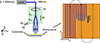 |
Figure 1 Left: Scheme of the SBIL lithography head. The binary beam splitter gratings G1 and G2 generate two collimated and coherent beams. The green marked area can rotate around the z-axis by angle γ. The mechanical setup above the microscope objective lens MO can be laterally shifted in the x–y-plane. Right: Principal scan-and-stitch process of scanning beam interference lithography. |
A general scan-and-stitch process of SBIL is shown in Figure 1, right. A writing spot with a few fringes scans along the fringe orientation. After every scan, the spot is shifted perpendicular to the scan direction. The shift is a multiple of the fringe period so that the next scan line is stitched to the already exposed area. This process is repeated until the entire substrate area is exposed. The high-precision fabrication of diffractive elements with SBIL requires precise adjustment of the lithography system. The various degrees of freedom of an SBIL lithography head are discussed below and the effects for the fabrication process in photo resist are explained.
2.1 Fringe period
The function and therefore the application range of a diffractive optical element depends largely on the grating period and is directly defined by the period of the fringe pattern of the writing spot. Therefore, it is essential to know the exact period before the exposure process. The period p is defined by the wavelength λ and incident angles θ1 and θ2 of the two interference beams as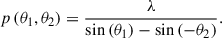 (1)
(1)
In the experimental setup, the fringe period can be adjusted by the position of G2. The propagation paths of the ±first orders from G1 define the distance between the two beams and therefore the incident angles θ1 and θ2 after the MO in the substrate plane. The displacement of G2 and the associated change in angle are shown in Figure 2. With θ1 = −θ2 = θ, the fringe period can then be expressed as![Mathematical equation: $$ p\left(\delta l\right)=\frac{\lambda }{2\cdot \mathrm{sin}\left(\mathrm{arctan}\left\{\frac{\delta l\cdot \mathrm{tan}\left[\mathrm{arcsin}\left(\frac{\lambda }{g}\right)\right]}{{f}^{\prime}}\right\}\right)} $$](/articles/jeos/full_html/2026/01/jeos20260016/jeos20260016-eq2.gif) (2)
(2)
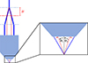 |
Figure 2 Scheme of grating shift to set the fringe pattern period. The grating G2 is shifted to change the incident angles and thus to set the period. θ1 and θ2 are defined from the bisector of the two interfering beam directions in the mathematically positive direction. |
where f′ is the focal length of MO and g the grating period of G1 and G2.
2.2 Fringe pattern orientation
Since SBIL is a scanning process, the orientation of the fringe pattern on the substrate must be well known relative to the direction of movement of the substrate’s positioning stage. As shown in Figure 3, the orientation depends on the orientation of the grating structures G1 and G2. If the substrate is scanned at an angle γ relative to the fringe pattern, the interference fringes are partially averaged over the finite size of the writing spot. This reduces the modulation of the intensity distribution in the photoresist and therefore lowers the contrast between the exposure maxima and minima. As a consequence, the minima of the exposure pattern can exceed the exposure threshold of the photoresist, so that regions which would remain unexposed at perfect fringe contrast become partially exposed. During development, these unintentionally exposed regions are also removed, which reduces the difference between exposed and unexposed areas. As a result, the resulting resist relief exhibits a smaller grating height. The magnitude of this effect strongly depends on the lateral dimensions of the writing spot [8].
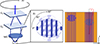 |
Figure 3 Scheme of the writing pattern rotation. G1 and G2 are rotated to align the orientation of the fringes. With a rotated pattern by angle γ, the contrast of the exposed areas in photo resist decreases significantly. |
Figure 3, right illustrates the effect of scanning with a rotated interference pattern: portions of the regions between adjacent fringes are unintentionally exposed, depending on the geometry of the writing spot. This results in a reduction of the effective grating height and consequently leads to lower diffraction efficiency.
2.3 Fringe pattern tilt
The two interference beams can be shifted laterally to the optical axis in two different directions δx and δy. That causes a tilt of the fringe pattern in the focal plane of the MO lens (see Fig. 4). The tilt of the fringe pattern is defined by the angle β between the substrate normal and the bisector of the two interfering beam directions, as illustrated in Figure 4. The fringe period p on the substrate then changes to (3)
(3)
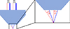 |
Figure 4 Scheme of the fringe pattern tilt in x-direction. Shifting the two beams by δx relatively, a tilt of βx of the writing pattern is induced. |
with θ1 = −θ2 = θ. For a large numerical aperture of the MO lens, the relation between the lateral shift in the pupil and the resulting propagation follows from the Abbe sine condition, which is fulfilled by well-corrected MOs. For the beams displaced by δx in the front focal plane of an objective with focal length f′, the propagation angle βx of the emerging collimated beam is given by![Mathematical equation: $$ {\beta }_x=\mathrm{arcsin}\left[\frac{\delta x}{{f}^\mathrm{\prime}}\right]. $$](/articles/jeos/full_html/2026/01/jeos20260016/jeos20260016-eq4.gif) (4)
(4)
This equation also applies to shifts in the y-direction.
Even if the change in period due to tilting is only slight, this degree of freedom plays an important role with regard to the illumination of non-planar substrates and thus represents an essential degree of freedom.
2.4 Scan-and-stitch process
In SBIL, large-area gratings are fabricated by translating the substrate through a localized interference field while the photoresist is continuously exposed. The substrate is scanned along the x-direction, while adjacent scan lines are stitched together in the y-direction. Mechanical positioning errors during scanning or stitching lead to local displacements of the recorded interference fringes and therefore introduce wavefront errors in the fabricated grating structure.
The interference pattern used for exposure forms a periodic intensity distribution. For a linear grating with period p, the interference intensity can be written as![Mathematical equation: $$ I(y)={I}_0\left\{1+\mathrm{cos}\left[\phi (y)\right]\right\}, $$](/articles/jeos/full_html/2026/01/jeos20260016/jeos20260016-eq5.gif) (5)
(5)
where I0 denotes the mean intensity and φ(y) is the spatial phase of the interference pattern. For an ideal grating the phase is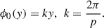 (6)
(6)
The phase φ(y) therefore determines the position of the maxima and minima of the intensity pattern that are recorded in the photoresist. Any displacement of the substrate during exposure shifts the local fringe position and thereby modifies the recorded phase of the grating [9].
2.4.1 Scan-induced phase errors
During the exposure of a scan line the substrate moves along the x-direction, while the fringe positions are defined along y, as shown in Figure 5. If the stage exhibits a positioning error perpendicular to the grating lines, denoted by Δyscan(x), the recorded interference pattern is shifted locally. This displacement introduces a phase deviation (7)
(7)
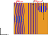 |
Figure 5 Sketch of the scan-and-stitching error. Positioning errors Δyscan while scanning the photoresist results in contrast loss and deviations of the linear grating. Stitching errors Δystich (red marked area) will result in phase jumps of the linear grating element. |
The resulting intensity distribution recorded in the photoresist becomes![Mathematical equation: $$ {I}_{\mathrm{scan}}\left(y,x\right)={I}_0\left[1+\mathrm{cos}\left({ky}+{k}\enspace \Delta {y}_{\mathrm{scan}}(x)\right)\right]. $$](/articles/jeos/full_html/2026/01/jeos20260016/jeos20260016-eq8.gif) (8)
(8)
Thus, positioning errors of the scanning stage directly translate into phase distortions of the recorded grating pattern. A phase error in the grating profile leads to a corresponding phase shift of the diffracted optical field.
The wavefront error W is the optical path difference. A first diffraction order with an illumination wavelength λassociated with a phase deviation Δφ results in (9)
(9)
In combination with equation (7), both relations yields the wavefront error induced by scan positioning errors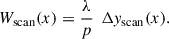 (10)
(10)
This relation shows that nanometer-scale positioning errors during scanning lead to wavefront errors of comparable magnitude in the diffracted beam.
2.4.2 Stitch-induced phase discontinuities
In addition to continuous scan errors, discrete phase discontinuities may occur at the boundaries between adjacent scan lines in the stitching direction y. If two neighboring scan lines are displaced by a lateral offset Δystitch, the interference pattern recorded in the photoresist exhibits a phase jump (11)
(11)
For a grating aperture composed of N stitched scan lines, the resulting wavefront error can be expressed as (12)
(12)
where H(y − yi) denotes the Heaviside function marking the location yi of each stitching boundary. These phase discontinuities introduce local phase steps or tilts in the diffracted wavefront, which reduce the coherent diffraction efficiency and increase the overall wavefront error of the optical element.
3 Experimental setup
The experimental setup is divided into three primary parts (Fig. 6): the lithography head, the FrObSy and the nanopositioning machine NPMM-200 [7]. The lithography head is mounted on a high stable and damped frame made of Zerodur and is decoupled of the movable stage itself. The FrObSy is placed and fixed on the movable stage of the NPMM-200.
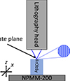 |
Figure 6 Scheme of the experimental setup. The fringe observation system (FrObSy) is placed on the stage of the NPMM-200. The lithography head is mounted in a high stable and damped frame made of Zerodur. The two exposure beams interfere in the focal plane of the observation system instead of a substrate. |
3.1 Lithography setup
The exposure laser is a fiber coupled Toptica Topmode 405 with a wavelength of 405 nm and a fiber output power adjustable up to 65 mW. The laser beam has a Gaussian beam profile (TEM00) with approx. 0.5 mm diameter. Behind the fiber output, the laser beam is collimated and then reflected by a 45° mirror. G1 and G2 are binary phase grating made of SiO2 with a period of p = 1 μm and a diffraction efficiency of approx. 40% for the ±first orders. The distance δl between G1 and G2 can be set manually from l1 = 2.5 mm to l2 = 12 mm with a maximum range of δlmax = 9.5 mm. With the Olympus microscope objective lens (UMPlanFI) with a numerical aperture of 0.8 (MO) and a focal length fMO = 3.6 mm, the two beams interfere in the focal plane, where the FrObSy is placed. Due to the electrical sliding contacts, the entire mount of the gratings can be rotated by a rotary drive up to 360° to adjust the orientation γ of the fringe pattern in the focal plane of MO. The shifts δx and δy can be performed by lateral actuators (see Fig. 7).
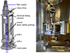 |
Figure 7 Left: Mechanical design of the SBIL lithography head. Right: Picture of the experimental setup, inserted in the mechanical mount of the positioning stage. |
3.2 The NPMM-200
The nanopositioning and measuring machine NPMM-200 [10] is a stage with nanometer positioning accuracy and a travel range of 200 × 200 × 25 mm3 (x, y, z). Six interferometers measure the six degrees of freedom. Except for the rotation around the z-axis, the axis in x, y, z direction and the rotational degrees of freedom rx and ry of the movable platform are controlled by actuators in the single digit nanometer range. The positioning stage is located in a large aluminum chamber, shown in Figure 8, left. This prevents the system from environmental disturbances, such as air and temperature fluctuations and dust particles. The mounting frame for the lithography head is made of Zerodur and is decoupled from the movable platform, as illustrated in Figure 8, right. This machine is a mandatory part of this work. As a reference system for FrObSy, the combination enables the high performance of the calibration and alignment procedures.
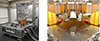 |
Figure 8 Left: The NPMM-200 in the experimental lab. For measurements and fabrication processes, the aluminum chamber will be closed. Right: Movable platform and the mounting frame. The laser beams (red marked) are reflected by a mirror corner made of optically smooth, polished Zerodur. Below the platform, three additional interferometer signals are reflected from the rear of a highly polished Zerodur surface. |
3.3 Fringe observation system
The FrObSy is the key tool to calibrate and align the described SBIL lithography head from Section 3.1. The mathematical and physical principle of the experimental evaluation with FrObSy is based on the carrier-frequency method [11] and the detour phase principle [12].
3.3.1 Fundamental principles
In the detour phase principle, the measured interferogram in one dimension y can be written as![Mathematical equation: $$ I(y)=a(y)+b(y)\mathrm{cos}\left[\phi (y)+{k}_{\mathrm{c}}x\right], $$](/articles/jeos/full_html/2026/01/jeos20260016/jeos20260016-eq13.gif) (13)
(13)
where a(y) and b(y) are the non coherent intensity distributions, φ(y) denotes the object-induced phase, and kc = 2π/p is the spatial carrier wavenumber determined by the fringe period p.
When the fringes of the writing spot are shifted perpendicular to the fringe orientation by an amount Δy, the interferogram becomes![Mathematical equation: $$ I\left(y-\Delta y\right)=a\left(y-\Delta y\right)+b\left(y-\Delta y\right)\mathrm{cos}\left[\phi \left(y-\Delta y\right)+{k}_{\mathrm{c}}\left(y-\Delta y\right)\right]. $$](/articles/jeos/full_html/2026/01/jeos20260016/jeos20260016-eq14.gif) (14)
(14)
This transformation introduces an additional phase term (15)
(15)
which represents a pure phase offset Δϕ of the complex signal in the Fourier domain. This behaviour is a direct consequence of the detour-phase principle. Any lateral displacement of a periodic structure generates a corresponding linear phase shift in its diffracted orders. The fringes imposed in the carrier-frequency method constitute such a periodic structure with spatial frequency kc. Thus, their lateral displacement does not modify the physical optical path of the writing spot, but instead alters the phase of the spatial frequency component that is isolated during Fourier demodulation. Consequently, the phase offset observed in the carrier-frequency method is determined solely by the fringe period p and the amount of lateral shift Δy.
3.3.2 Data acquisition
An Olympus microscope objective lens (UMPlanFI) with a numerical aperture of 0.95 and an effective focal length of f = 1.8 mm is placed in the focal position of the lithography head instead of the substrate, as shown in Figure 9. After the MO, the beams are reflected by a tilted mirror. To image the fringes on the camera chip, a tube lens (TL) with a focal length of f′ = 200 mm is used. Then the lateral magnification factor ML is 111. The camera used is a Ximea MC124MG-SY-UB with a pixel pitch xpixel = 3.45 μm and a total sensor size of 14.2 mm × 10.4 mm. An image of the writing spot can be seen in Figure 9. In combination with the NPMM-200, the positioning of FrObSy is measured in six degrees of freedom, which enables high accuracy measurements and positioning.
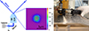 |
Figure 9 Optical setup of FrObSy. Left: The exposure beams interfere in the focal plane of the microscope objective lens. Inlet: An image of the writing spot is shown. Right: Experimental integration of the observation system, mounted on the platform of the NPMM-200. The distance between the objective of the lithography head and the objective of FrObSy is about 3 mm. |
The fringe motion is monitored over time. The single steps of the data evaluation are visualized in Figure 10. At first, the initial image is cropped to an area with 48 × 48 pixels (red rectangle). Then the 2D-Fourier transform is applied. The region of interest around the main frequency peak (rectangle marked in red) with 2 × 2 pixels is shifted to the 2D-Fourier center, i.e. to remove the carrier-frequency of the interference pattern. All other frequencies are set to zero to minimize noise signals. With the inverse Fourier-transform, the phase can be calculated from the real part and the imaginary part. The offset Δϕ of the wavefront is the mean value and represents the fringe movement. At the beginning of the measurement, an initial offset Δϕ is measured and defined as zero. To quantify the movement in nanometers, the period of the fringes has to be determined. Then the fringe movement Δr can be calculated by (16)
(16)
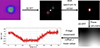 |
Figure 10 Evaluation steps of the fringe observation system. The carrier-frequency method is applied to a region of interest in the camera image (indicated by the red rectangle). The main frequency peak of the 2D FFT is shifted to the center of the Fourier space and all other frequencies are set to zero. After inverse 2D FFT, the phase can be calculated from the imaginary part and the real part. The wavefront offset, which corresponds to the fringe movement of the fringe pattern, then can be calculated by the mean value. |
where Δϕ is the measured phase with the carrier-frequency method and p is the period of the fringe pattern in nanometers. The determination of p is described in Section 4.2. The data acquisition rate (including camera image acquisition and phase calculation) is about 30 Hz. The integration time of the camera is set to 8 ms. The data sets are evaluated with the python developer environment ITOM [13].
4 Alignment of an SBIL system
For the alignment of the SBIL system in Section 3.1, we created a well defined alignment protocol, which covers all necessary degrees of freedom to align the setup and to characterize the positioning errors for the scan-and-stitch process. The alignment protocol is visualized in Figure 11. The different steps are explained in detail in the following sections.
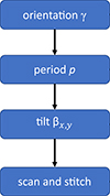 |
Figure 11 Scheme of the alignment process. |
4.1 Alignment of the fringe pattern orientation
At first, the orientation γ of the fringe pattern is aligned. The NPMM-200 axis will move along the x-axis with a linear trajectory Δx. During movement, the fringes on the camera shift. As illustrated in Figure 12, this leads to a measurable phase offset Δϕ (see Eq. (15)) depending on γ. Figure 13 shows the measurement data of the offset over time.
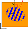 |
Figure 12 Scheme of the determination of fringe pattern orientation. |
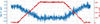 |
Figure 13 Measurement of the fringe movement Δϕ while moving the stage along x-axis with Δx over time. Two steps forward and backward with 400 nm with a velocity of 27 nm/s are performed. |
The measurement of Δϕ over Δx is shown in Figure 14. A linear function is fitted to Δϕ(Δx) to determine the gradient mx. The fringe pattern orientation γ can be calculated by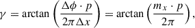 (17)
(17)
where p is the period of the fringe pattern.
At this point, the fringe pattern period p and the pattern rotation by the rotary drive are still not known with sufficient accuracy, which prevents a direct determination of the orientation angle γ. To overcome this, the lithography head is incrementally rotated by δγ while monitoring the phase Δϕ(Δx). The rotation measurement is continued until the measured gradient mx, representing the phase change per displacement Δx, vanishes. A zero gradient indicates that the scan direction is orthogonal to the fringe orientation, and thus the residual orientation error of the lithography head has been eliminated. Figure 15 shows a measurement with sufficiently minimized gradient mx = 0.018 mrad/mm with a fitting uncertainty of ±0.015 mrad/mm.
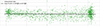 |
Figure 15 Measurement of the fringe movement Δϕ over Δx. The orientation angle γ is aligned to minimize the gradient mx of the linear fit. |
4.2 Fringe period determination
With the aligned orientation, the stage will be moved with well known steps Δy perpendicular to the fringe pattern orientation. In Figure 16, five steps with 50 nm and with a velocity νy = 1 μm were performed over a period of 90 s to characterize the difference of the measurement accuracy of FrObSy during dynamic stage movements and static positions.
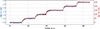 |
Figure 16 Measurement of Δϕ and the stage movement Δy perpendicular to the fringe orientation over time. Five steps were performed over a total period of 90 s. |
The period can then be calculated by Eq. (15) by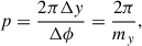 (18)
(18)
where my is the gradient of the linear fit in Figure 17. The period was determined to p = 558.2 nm (±1 nm). This result will be validated with exposure experiments in photo resist (see Section 4.5). In order to estimate the accuracy of the phase measurement, the phase offset Δϕ is converted into an equivalent lateral displacement using Eq. (16).The resulting fringe movement Δr can then be directly compared to the stage position signal Δy. Figure 18 shows the difference between both signals as well as the corresponding low-pass filtered data over time.
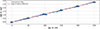 |
Figure 17 Movement of the fringes Δϕ over the stage movement Δy. The fringe period p can be determined from the gradient my of a linear fit of the measurement data. |
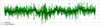 |
Figure 18 Difference between the measured fringe movement Δϕ in nanometer and the y-interferometer signal Δy in order to evaluate the measurement accuracy of the fringe observation system. |
A striking feature of the measurement is the presence of high-frequency oscillations with an RMS value of approximately 4.06 nm. These oscillations originate from residual tilting of the positioning stage. Although the rotational degrees of freedom rx and ry about the x- and y-axes are actively controlled, they exhibit a residual control error of approximately ±70 nrad. Consequently, the stage shows a slight oscillatory tilt during the measurement. This tilt leads to a lateral displacement of the entrance pupil of the MO. The magnitude of this displacement depends on the optical path height hopt, which corresponds to the effective vertical distance between the rotation center of the stage and the entrance pupil of the MO lens. For the present setup, this distance is approximately (19)
(19)
A small angular deviation rx therefore produces a lateral displacement (20)
(20)
For rx ≈ ±70 nrad this results in a displacement of approximately ±6 nm at the entrance pupil of the objective. This displacement directly shifts the recorded interference fringes and therefore appears as an additional phase offset in the measured signal Δϕ.
In addition to the high-frequency oscillations, the low-pass filtered data reveals slower phase fluctuations with an RMS of approximately 1.3 nm. These fluctuations are mainly attributed to thermally induced variations of the refractive index along the optical path. Small air turbulences cause local changes in the refractive index, which modify the optical path length of the interfering exposure beams. As a consequence, the relative phase between the beams varies slightly over time, resulting in a slow drift of the interference fringes.
4.3 Fringe pattern tilt calibration
In order to characterize the tilt of the fringe pattern, a scan along the z-axis has to be performed. A long-range scan along z is performed in order to visualize an aerial image of the two writing beams. Figure 19 illustrates how aerial images are generated from individual camera images using a 2D volume cut. For each step zi, an image of the writing pattern is captured and the offset value Δϕ is tracked, as shown in Figure 20.
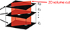 |
Figure 19 Visualization of the z scan to generate the aerial images from the camera images via 2D volume cut. |
 |
Figure 20 Scheme of the fringe pattern tilt in x-direction. In order to determine the fringe pattern tilt βx a z-scan will be performed. |
The 2D volume cut of two image stacks with different tilts are shown in Figure 21. The right cross section shows a tilted writing pattern with approx. 21°. After movement of the lateral actuator in δy, the writing pattern is tilted close to the vertical position, as shown in Figure 21, left.
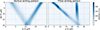 |
Figure 21 Aerial image of two different tilted writing patterns. An image scan along the z-axis was performed and the resulting two dimensional linecut was then plotted. Left: Vertical writing pattern. Right: Tilted writing pattern with approx. β = 21°. |
In order to quantify the tilt β, a high resolution scan with 2 μm range and a step size of 20 nm is performed close to the focus position of the writing pattern (see Fig. 22). The fringe shift Δϕ exhibits a superimposed periodic modulation as a function of the axial displacement Δz. This modulation arises from the transverse sampling of the fringes during measurement along z, as the tilt causes the minima and maxima to be intersected alternately. Therefore, the behavior of the offset measurement can be described as a superposition of a linear shift and the interference intensity distribution as (21)
(21)
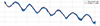 |
Figure 22 High resolution scan of the writing pattern with 2 μm scan range and 20 nm step size in order to quantify the writing pattern tilt β. While scanning Δz, the fringe movement Δϕ of the fringe pattern is tracked. A functional fit is then applied to determine the gradient of the linear shift of the fringes and therefore to determine β. |
mz is the linear gradient of the offset shift, a is the amplitude of the intensity modulation, ω the spatial frequency of the modulation, φ0 the initial phase of the modulation and c an initial phase offset. The gradient mz is determined by performing a fit with Eq. (21). The gradient is then used to calculate the tilt angle with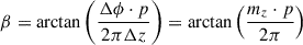 (22)
(22)
to βx = -1.894°. However, it should be noted here that the period must be redetermined for each change in the tilt of the writing pattern in order to determine the phase offset in nanometers accurately and thus the actual tilt. The fringe pattern tilt calibration can then be repeated for the other tilt direction βy.
4.4 Evaluation of positioning errors
In a last step of calibration, the positioning error occuring during the scan-and-stitch process is characterized. The platform is translated such that the entire camera field of view is illuminated. Within an area of 14 × 14 μm2, scanning is performed along the x-axis at a velocity of 10 μm/s, followed by stitching with an offset of three fringe periods. The FrObSy is mounted on the platform with a 45° rotation, resulting in the fringes being imaged at an angle of approximately 45°, too (see Fig. 23, left). Every 10 ms, an image of the current position of the writing point is captured on the camera and the recorded image stack is combined into a single image. The recorded pattern is subsequently analyzed using the carrier-frequency method, as illustrated in Figure 10. A Zernike polynomial fit is then applied to the inner circle of the reconstructed wavefront to remove remaining tip and tilt components. The resulting positioning error is shown in Figure 23, right. Positioning errors of approx. 75 nm peak-to-valley with an RMS of 15.6 nm can be observed. The errors are caused by vibrational errors of the positioning stage with a frequency of approx. 20 Hz. These errors lead to observable deviations in each individual scan line.
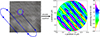 |
Figure 23 Evaluation of positioning errors during the scan-and-stitch process. The fringe observation system is moved with 10 μm/s in x-direction and is stitched with an overlap of three fringes in y-direction. The recorded image stack is combined into a single image. The wavefront error of the recorded pattern is calculated by using the carrier-frequency method. A Zernike polynomial fit is applied to the inner circle of the reconstructed wavefront error to remove remaining tip and tilt components. |
4.5 Exposure results
To evaluate the previously achieved alignment and calibration, exposure tests were performed in positive photo resist (AZ MIR 701 from MicroChemicals) with a fiber output power of 1 mW. Figure 24 shows three exposures with different scan velocities of 0.5, 0.2 and 0.1 mm/s, each consisting of two scan passes, one forward and one backward without overlap.
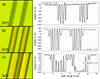 |
Figure 24 Microscope images and corresponding atomic force microscope (AFM) measurements for photo resist structures with different scan velocities ν. (a) Underexposed structures with ν = 0.5 mm/s, (b) well exposed structures with ν = 0.2 mm/s, (c) overexposed structures with ν = 0.1 mm/s. |
In Figure 24a, a clearly underexposed structure is observed. Nevertheless, the structure exhibits very good contrast during scanning, as the upper region of the grating structure remains at the level of the unexposed resist. Figure 24b shows nearly optimal grating structures with a well-defined duty cycle. In this case, the structural period was determined to be 556.7 nm (±3 nm) with a structure height of 358 nm ± 2 nm. Figure 24 c demonstrates overexposure of the photo resist. The Gaussian intensity distribution of the writing pattern is clearly visible, as indicated by the varying height of the resist profile. These results served as the basis for the first stitching experiments in photo resist with a scan velocity ν = 0.3 mm/s. An AFM measurement is presented in Figure 25. For each stitching step, two fringes of the writing spot were superimposed. The consistently high contrast across the measured region is clearly evident, as the upper surface of the patterned structures remains at the same height as the unexposed areas.
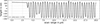 |
Figure 25 AFM measurement of a first scan-and-stitch process in photo resist. |
5 Conclusion
A new calibration and alignment tool for SBIL system was developed. A FrObSy, consisting of a compact microscope that is positioned on a nanopositioning machine, images the writing pattern of a specific SBIL lithography head onto a camera. The motion of the fringes is quantified via carrier-frequency method. Different measurement approaches for the quantitative evaluation of fringe dynamics were presented. A protocol for the adjustment and calibration process was developed to characterize various degrees of freedom of the lithography head. Starting with the determination and alignment of the fringe orientation γ, the writing pattern was aligned so that the fringes were parallel to the scan direction, thus ensuring good contrast during exposure in photo resist. Subsequently, the fringe period p = 558.2 nm (±1 nm) could be determined by measuring the fringe displacement. Furthermore, the tilts of the writing pattern βx,y were characterized via aerial images and quantified by high-resolution measurements along the focus of the exposure beams with a tilt of 1.894°. Subsequently, the positioning error during the scan-and-stitch process was determined. For this approach, a classic SBIL trajectory was traversed with the observation system and the recorded fringe pattern was analyzed using the carrier-frequency method. With 75 nm peak-to-valley and an RMS of 15.6 nm the errors lead to observable deviations in each individual scan line. Finally, initial exposure tests were carried out in positive photo resist to demonstrate the successful calibration and adjustment of the lithography head. The photo resist was exposed at different scanning velocities, and it was observed that the ridges of the linear structures exhibited no material loss, indicating an optimal contrast of the exposure pattern. Furthermore, the structural period was determined to be p = 556.7 nm (±3 nm), which is in excellent agreement with the measurements obtained using FrObSy with p = 558.2 nm (±1 nm). In future work, the FrObSy will be employed to calibrate an in-situ feedback and compensation system for the presented lithography head. All relevant degrees of freedom will be detected and the corresponding control loops will be designed accordingly. This approach aims to minimize the positioning errors identified in this study and thereby significantly improve the fabrication of linear gratings using SBIL.
Funding
This work was supported by the German Research Foundation (Deutsche Forschungsgemeinschaft, DFG), grant no. 465642714. The nanopositioning and measuring machine NPMM-200 was funded by the Deutsche Forschungsgemeinschaft (DFG, German Research Foundation) – 267094782.
Conflicts of interest
The authors declare that they have no competing interests to report.
Data availability statement
Data underlying the results presented in this paper are not publicly available at this time but may be obtained from the authors upon reasonable request.
Author contribution statement
Conceptualization K.T., J.R., I.O., C.P., T.H., O.S., E.M., T.K. and S.R.; Methodology C.P., T.H., O.S., E.M., T.K. and S.R.; Software, K.T., I.O. and J.R.; Investigation K.T., J.R., I.O. and C.P.; Writing – Original Draft Preparation K.T.; Writing – Review & Editing K.T., J.R., I.O., C.P., T.H., O.S., E.M., T.K. and S.R.; Project administration T.H., O.S., E.M., T.K. and S.R.; Funding acquisition T.H., O.S., E.M.
Acknowledgments
We would like to thank Holger Ruehl for his assistance in characterizing the exposed gratings.
References
- Chen Y., Konkola P., Heilmann R.K., Schattenburg M.L. (2002) Nanometer-accurate grating fabrication with scanning beam interference lithography, Proc. SPIE 4936, 126–134. https://doi.org/10.1117/12.469431. [Google Scholar]
- Chen Y., Konkola P., Heilmann R.K., Joo C., Schattenburg M.L. (2002) Beam alignment for scanning beam interference lithography, J. Vac. Sci. Technol. B 20, 3071–3074. https://doi.org/10.1116/1.1523402. [Google Scholar]
- Zhou Q., Oh J., Kim D., Suryani I.O., Han R., Kang S. (2026) Control of scanning beam interference lithography by real-time compensation of scan angle error through acoustooptic modulation and phase-shift grating interferometry for large area nanostructuring, Micro Nano Manuf. 2. https://doi.org/10.1007/s44374-025-00009-2. [Google Scholar]
- Feigel A., Kotler Z., Sfez B. (2002) Scalable interference lithography alignment for fabrication of three-dimensional photonic crystals, Opt. Lett. 27, 746–748. https://doi.org/10.1364/OL.27.000746. [Google Scholar]
- van Soest G., van Wolferen H.A.G.M., Hoekstra H.J.W.M., Worhoff K., Lambeck P.V. (2005) Laser interference lithography with highly accurate interferometric alignment, Jpn. J. Appl. Phys. 44, 6568–6570. https://doi.org/10.1143/JJAP.44.6568. [Google Scholar]
- Gao Q., Li Y., Zhong L., Li Y. (2025) Global alignment reference strategy for laser interference lithography pattern arrays, Microsyst. Nanoeng. 11, 4. https://doi.org/10.1038/s41378-025-00889-4. [Google Scholar]
- Jäger G., Manske E., Hausotte T., Müller A., Balzer F. (2016) Nanopositioning and nanomeasuring machine NPMM-200 – a new powerful tool for large-range micro- and nanotechnology, Surf. Topogr. Metrol. Prop. 4, 034004. https://doi.org/10.1088/2051-672X/4/3/034004. [Google Scholar]
- Li Y., Jiang S., Chen X., Liu Z.,Wang W., Song Y., Bayanheshig. (2023) Accurate measurement and adjustment method for interference fringe direction in a scanning beam interference lithography system, Opt. Express. https://doi.org/10.1364/OE.485488. [Google Scholar]
- Li W., et al. (2025) Controlling the wavefront aberration of a large-aperture and high-precision holographic diffraction grating, Light Sci. Appl. https://doi.org/10.1038/s41377-025-01785-2. [Google Scholar]
- Schober C., Pruss C., Herkommer A., Osten W. (2020) The NPMM-200: large area high resolution for freeform surface measurement, Proc. SPIE. https://doi.org/10.1117/12.2564918. [Google Scholar]
- Takeda M., Ina H., Kobayashi S. (1982) Fourier-transform method of fringe-pattern analysis for computer-based topography and interferometry, J. Opt. Soc. 72. https://doi.org/10.1364/JOSA.72.000156. [Google Scholar]
- Brown B.R., Lohmann A.W. (1966) Complex spatial filtering with binary masks, Appl. Opt. 5, 967–969. https://doi.org/10.1364/AO.5.000967. [Google Scholar]
- Gronle M., Lyda W., Wilke M., Kohler C., Osten W. (2014) itom: an open source metrology, automation, and data evaluation software, Appl. Opt. 53, 2974–2982. https://doi.org/10.1364/AO.53.002974. [Google Scholar]
All Figures
|
Figure 1 Left: Scheme of the SBIL lithography head. The binary beam splitter gratings G1 and G2 generate two collimated and coherent beams. The green marked area can rotate around the z-axis by angle γ. The mechanical setup above the microscope objective lens MO can be laterally shifted in the x–y-plane. Right: Principal scan-and-stitch process of scanning beam interference lithography. |
| In the text | |
|
Figure 2 Scheme of grating shift to set the fringe pattern period. The grating G2 is shifted to change the incident angles and thus to set the period. θ1 and θ2 are defined from the bisector of the two interfering beam directions in the mathematically positive direction. |
| In the text | |
|
Figure 3 Scheme of the writing pattern rotation. G1 and G2 are rotated to align the orientation of the fringes. With a rotated pattern by angle γ, the contrast of the exposed areas in photo resist decreases significantly. |
| In the text | |
|
Figure 4 Scheme of the fringe pattern tilt in x-direction. Shifting the two beams by δx relatively, a tilt of βx of the writing pattern is induced. |
| In the text | |
|
Figure 5 Sketch of the scan-and-stitching error. Positioning errors Δyscan while scanning the photoresist results in contrast loss and deviations of the linear grating. Stitching errors Δystich (red marked area) will result in phase jumps of the linear grating element. |
| In the text | |
|
Figure 6 Scheme of the experimental setup. The fringe observation system (FrObSy) is placed on the stage of the NPMM-200. The lithography head is mounted in a high stable and damped frame made of Zerodur. The two exposure beams interfere in the focal plane of the observation system instead of a substrate. |
| In the text | |
|
Figure 7 Left: Mechanical design of the SBIL lithography head. Right: Picture of the experimental setup, inserted in the mechanical mount of the positioning stage. |
| In the text | |
|
Figure 8 Left: The NPMM-200 in the experimental lab. For measurements and fabrication processes, the aluminum chamber will be closed. Right: Movable platform and the mounting frame. The laser beams (red marked) are reflected by a mirror corner made of optically smooth, polished Zerodur. Below the platform, three additional interferometer signals are reflected from the rear of a highly polished Zerodur surface. |
| In the text | |
|
Figure 9 Optical setup of FrObSy. Left: The exposure beams interfere in the focal plane of the microscope objective lens. Inlet: An image of the writing spot is shown. Right: Experimental integration of the observation system, mounted on the platform of the NPMM-200. The distance between the objective of the lithography head and the objective of FrObSy is about 3 mm. |
| In the text | |
|
Figure 10 Evaluation steps of the fringe observation system. The carrier-frequency method is applied to a region of interest in the camera image (indicated by the red rectangle). The main frequency peak of the 2D FFT is shifted to the center of the Fourier space and all other frequencies are set to zero. After inverse 2D FFT, the phase can be calculated from the imaginary part and the real part. The wavefront offset, which corresponds to the fringe movement of the fringe pattern, then can be calculated by the mean value. |
| In the text | |
|
Figure 11 Scheme of the alignment process. |
| In the text | |
|
Figure 12 Scheme of the determination of fringe pattern orientation. |
| In the text | |
|
Figure 13 Measurement of the fringe movement Δϕ while moving the stage along x-axis with Δx over time. Two steps forward and backward with 400 nm with a velocity of 27 nm/s are performed. |
| In the text | |
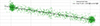 |
Figure 14 Measurement of the fringe movement Δϕ over stage movement Δx, corresponding to Figure 13. |
| In the text | |
|
Figure 15 Measurement of the fringe movement Δϕ over Δx. The orientation angle γ is aligned to minimize the gradient mx of the linear fit. |
| In the text | |
|
Figure 16 Measurement of Δϕ and the stage movement Δy perpendicular to the fringe orientation over time. Five steps were performed over a total period of 90 s. |
| In the text | |
|
Figure 17 Movement of the fringes Δϕ over the stage movement Δy. The fringe period p can be determined from the gradient my of a linear fit of the measurement data. |
| In the text | |
|
Figure 18 Difference between the measured fringe movement Δϕ in nanometer and the y-interferometer signal Δy in order to evaluate the measurement accuracy of the fringe observation system. |
| In the text | |
|
Figure 19 Visualization of the z scan to generate the aerial images from the camera images via 2D volume cut. |
| In the text | |
|
Figure 20 Scheme of the fringe pattern tilt in x-direction. In order to determine the fringe pattern tilt βx a z-scan will be performed. |
| In the text | |
|
Figure 21 Aerial image of two different tilted writing patterns. An image scan along the z-axis was performed and the resulting two dimensional linecut was then plotted. Left: Vertical writing pattern. Right: Tilted writing pattern with approx. β = 21°. |
| In the text | |
|
Figure 22 High resolution scan of the writing pattern with 2 μm scan range and 20 nm step size in order to quantify the writing pattern tilt β. While scanning Δz, the fringe movement Δϕ of the fringe pattern is tracked. A functional fit is then applied to determine the gradient of the linear shift of the fringes and therefore to determine β. |
| In the text | |
|
Figure 23 Evaluation of positioning errors during the scan-and-stitch process. The fringe observation system is moved with 10 μm/s in x-direction and is stitched with an overlap of three fringes in y-direction. The recorded image stack is combined into a single image. The wavefront error of the recorded pattern is calculated by using the carrier-frequency method. A Zernike polynomial fit is applied to the inner circle of the reconstructed wavefront error to remove remaining tip and tilt components. |
| In the text | |
|
Figure 24 Microscope images and corresponding atomic force microscope (AFM) measurements for photo resist structures with different scan velocities ν. (a) Underexposed structures with ν = 0.5 mm/s, (b) well exposed structures with ν = 0.2 mm/s, (c) overexposed structures with ν = 0.1 mm/s. |
| In the text | |
|
Figure 25 AFM measurement of a first scan-and-stitch process in photo resist. |
| In the text | |
Current usage metrics show cumulative count of Article Views (full-text article views including HTML views, PDF and ePub downloads, according to the available data) and Abstracts Views on Vision4Press platform.
Data correspond to usage on the plateform after 2015. The current usage metrics is available 48-96 hours after online publication and is updated daily on week days.
Initial download of the metrics may take a while.