| Issue |
J. Eur. Opt. Society-Rapid Publ.
Volume 22, Number 1, 2026
PLASMONICA Collection
|
|
|---|---|---|
| Article Number | 37 | |
| Number of page(s) | 7 | |
| DOI | https://doi.org/10.1051/jeos/2026020 | |
| Published online | 12 May 2026 | |
Short Communication
Tunable modulation frequency in photo-acoustic spectroscopy towards precise discrimination of resonant modes in nanostructures on absorbing substrates
1
Sapienza University of Rome, Department SBAI, Rome 00161, Italy
2
École Nationale Supérieure de Techniques Avancées, 91120 Palaiseau, France
3
Optoelectronics Research Centre, Physics Unit, Tampere University, Korkeakoulunkatu 3, 33720 Tampere, Finland
* Corresponding author: This email address is being protected from spambots. You need JavaScript enabled to view it.
Received:
26
October
2025
Accepted:
25
February
2026
Abstract
Scattering-free assessment of resonantly absorbed electromagnetic field is highly important in nano-photonics and plasmonics: nanostructures and metamaterials can be tailored to optimize absorption for applications spanning from solar cells to efficient gas sensing. Photo-acoustic technique converts absorption-induced periodic heating in an acoustic signal, giving powerful means of characterizing absorption in scattering-free and non-destructive way. In this work, we use a widely tunable laser and tunable modulation frequency to perform photo-acoustic experiment on nanowire ensembles. We study absorption in two samples: semiconductor and semiconductor-plasmonic nanowires, both vertically standing on absorbing substrates. Increasing the modulation frequency from 54 Hz to 1225 Hz leads to a more precise discrimination of the resonant absorption modes of the nanowires, against the absorbing substrate. We show this behavior for GaAs-based nanowires in the near-infrared range. Moreover, in the hybrid sample, the asymmetric Au layer leads to extrinsic chiral response in the whole wavelength range.
Key words: Photo-acoustic spectroscopy / Plasmonics / Nanostructures / Nanowires / Absorption
© The Author(s), published by EDP Sciences, 2026
 This is an Open Access article distributed under the terms of the Creative Commons Attribution License (https://creativecommons.org/licenses/by/4.0), which permits unrestricted use, distribution, and reproduction in any medium, provided the original work is properly cited.
1 Introduction
Nanostructured materials can be engineered to exhibit specific resonant absorption modes, optimizing the behavior of nanodevices from photodetectors [1] to molecular sensors [2]. Nanoscale structures are usually deposited on a much more robust substrate layer. This layer, though, interferes with an accurate evaluation of the sample absorption or its resonances. Photo-acoustic spectroscopy (PAS) is a non-invasive, contactless, photo-thermal technique that allows for a direct measurement of the sample’s absorption without the scattering influence. In PAS, light, modulated at a frequency f, excites the sample in a closed cell. This periodic sample absorption leads to periodic heating, creating thermal waves that can be detected by a sensitive microphone. The electric signal is then compared with the modulation reference through a lock-in amplifier. Such extracted PAS signal depends on the sample material properties: absorption and thermal diffusivity. For optically and thermally thick samples, the absorption coefficient spectrum can be calculated from the normalized PAS amplitude [3], while the PAS spectrum follows the form of the absorbance. By varying the chopper frequency, different depths along the sample’s height can be probed. This tool was shown to be a promising in characterization of optical and photo-thermal properties of absorbing materials on substrates, being those nanoparticles [4], thin films [5], periodic plasmonic structures [6] or ensembles of nanowires [7].
In PAS, the detected absorption signal arises from the material volume limited by the thermal diffusion length, which scales with the modulation frequency as  . Therefore, increased modulation frequencies allow measurements of upper zones of the samples that can be nanostructured to exhibit resonant absorption modes. Previously, we qualitatively showed that an increase in modulation frequency can be used to access the resonant absorption in nanowires (NW) against their substrates, even if both strongly absorb in the same wavelength range. In Ref. [8], we used white light lamp source to excite GaAs-based NW on Si substrate, and we monitored the difference of the NW signal with respect to the one of the substrate, i.e. normalized PAS signal. When we changed the modulation frequency from 27 Hz to 225 Hz, the resonant leaky-waveguide modes appeared in the normalized signal. However, due to the photo-acoustic cell design, the amplitude of the PAS signal decreases with the increase of f [9], and the signal to noise ratio of the normalized signal deteriorates. Hence, to eliminate the influence of the substrate, modern PAS set-ups require the power tunability of the excitation light beam. Moreover, polarization control of the absorption in asymmetric NW in a wide wavelength range can be assessed if the lamp source is replaced by a widely tunable laser.
In this work, we apply PAS tunability in terms of light wavelength, and beam modulation frequency, to push the limits of the mode detection in vertically standing NW ensembles. We investigate two samples: GaAs-based NWs, and the same sample asymmetrically covered by Au (2 out of 6 NW sidewalls). The semiconductor-only sample supports a leaky waveguide resonance at ~780 nm. We apply PAS with a laser, widely tunable in the (680–1000) nm range and in power, which allows us to access higher modulation frequency. The normalized absorption signal sharpens when f is changed from 54 Hz to 1225 Hz, as the influence of the substrate decreases. We further show that Au-covered sample exhibits extrinsic chirality in the whole wavelength range.
2 Materials and methods
Figure 1a shows schematic of the photo-acoustic set-up, with sketches of the two investigated samples. The photo-acoustic cell is positioned on a rotation/translation stage. The laser wavelength is tunable in the (680–1000) nm range (including tunable power), and the modulation frequency of the chopper frequency is tunable up to 2000 Hz. We enable the precise laser position on the sample by a microscope. In this work, the light is focused to around ~300 μm diameter.
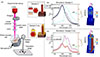 |
Fig. 1 (a) Photo-acoustic spectroscopy, allows for tunable polarization, power, modulation frequency, incidence angle; inset: schematic of the two samples. Both have diameter of 165 nm and height of 4.6 μm; Sample C-Au has two out of six sidewalls covered by 20 nm Au. (b) Simulation of a single NW of Sample C, in the air and standing on the Si substrate, and the 3D distribution of the absorption density at the resonance of 780 nm. The Si substrate widens the leaky waveguide mode resonance. (c) Simulation of a single NW covered by Au, and the 3D distribution of the absorption density at 850 nm. Here, the substrate strongly influences absorption as its parts contain absorbing material. |
The investigated samples are ensembles of vertically standing, coaxial GaAs-AlGaAs-GaAs core-shell-supershell NWs, grown by molecular beam epitaxy on p-Si(1 1 1) substrates. This process starts with lithography-free Si/SiOx patterns defining the nucleation sites for self-catalyzed growth of GaAs core [10]. Since the patterns were obtained by means of droplet epitaxy of GaAs nanocrystals, the final ensemble has randomly positioned NWs. The GaAs core growth results in predominantly defect free zincblende structure. Next, AlGaAs shell and GaAs supershell are grown using axial growth promoting conditions. As a result, the NW ensemble has density of 1 NW/μm2, and a good uniformity of geometric parameters, as shown by detailed statistical analysis of scanning electron microscope images in Ref. [7].
In the investigated Sample C, a single NW is 4.65 μm tall, and has the overall diameter of 165 nm, which contains 11.6 nm AlGaAs shell, and 5.9 nm GaAs supershell. The shell/supershell growth results in additional parasitic layers on the top of Si substrate (25 nm and 5 nm of AlGaAs and GaAs, respectively). The investigated Sample C-Au has the same semiconductor base as Sample C, on the top of which a thin Au layer was grown using electron beam evaporation. In order to break the symmetry in the Au-covered NW sidewalls, the Au flux was tilted for 14° angle with respect to the nanowire axis. This resulted in around 17 nm of Au on two out of six NW sidewalls. Samples of thinner NW diameters, fabricated by the same technique, were previously investigated by reflection spectroscopy [11].
Furthermore, we use finite-difference-time-domain simulations to predict the optical behavior of NWs in the same wavelength range. We employ a commercial 3D solver of Maxwell’s equations by Lumerical [12]. Complex refractive indices of GaAs and AlGaAs are taken from Ref. [13]. We use a broadband total-field-scattered-field source to excite a single NW in the air or on the substrate, under normal incidence. This method separates the power absorbed by the medium from the scattered one, which numerically mimics the photo-acoustic measurements, as shown later in the manuscript. The absorption cross-section is defined by a box of monitors surrounding the NW (200 nm × 200 nm × 6 μm); the absorption efficiency ηabs is then calculated by dividing the absorption cross-section with the geometric cross-section.
3 Results and discussion
A single GaAs NW with diameters in (60–200) nm range supports leaky resonant absorption modes below the GaAs bandgap [14]. Figure 1b shows such mode in a single NW of the Sample C, peaking at 780 nm; the inset plots 3D absorption density at that wavelength. When the NW is placed on the substrate, the same absorption cross-section box contains a small volume of the absorbing substrate material; nonetheless, the presence of the substrate leads to the background absorption, slightly modifying the spectral shape of the resonance. Sample C-Au is modelled by taking into account all Au material influences: the Au layer on the two sidewalls, the Au layer present on the substrate, including the NW shadowing effect, and a plasmonic “cap” on the top of the NW. This strongly reshapes the resonances of the semiconductor NW. In Figure 1c, the absorption is red-shifted for the NW with two sidewalls in the air; when such NW is placed on the substrate with Au, this substrate red-shifts and strongly increases the absorption. Finally, the hybrid semiconductor-plasmonic nanowire has a prominent absorption for wavelengths greater than the GaAs bandgap, i.e. in the (870–1000) nm range. Dashed lines in Figures 1b–1c present scattering cross-section spectra of a single NW, without and with Au; at these NW dimensions, they differ in the spectral position of the resonances [15]. Hence, trying to characterize the resonant absorption by performing extinction measurements would be misleading, especially in terms of ascribing the observed signal peaks to the electromagnetic field enhancement at the same wavelength, e.g. for improved sensing or heat transport at the nanoscale [16].
We next apply PAS to detect the resonant absorption modes in the two samples; as a reference, we use the substrate of the Sample C (Si, without Au). We excite them at normal incidence, with linear polarization, in the (680–1000) nm range, and tune the chopper frequency f. Figure 2a plots PAS signal amplitudes, normalized to the incident laser power, for Samples C, C-Au and the substrate. At 54 Hz, both nanostructured samples absorb more than the substrate, with no particular resonant features. In our previous work [8], we observed the resonant absorption modes in similar samples at 225 Hz. In this work, the laser allows for wider power tunability, so we choose higher frequencies of 408 Hz and 625 Hz. At both frequencies, starting from wavelength of 820 nm, we observe a distinct absorption drop for Sample C; moreover, in that range, the difference between this sample and the substrate decreases. This does not happen for Sample C-Au, as it absorbs in the whole investigated spectral range; instead, for wavelengths larger than 840 nm, the absorption is increased with respect to both substrate and Sample C. In this sample, apart from the Au layer on the NW, Au layer on the substrate also contributes to the absorption signal.
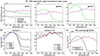 |
Fig. 2 (a) PAS signal amplitude of samples C, C-Au and the substrate (without Au), excited at normal incidence and modulated with 54Hz, 408 Hz and 625 Hz chopper frequency; the excitation is at normal incidence with linear polarization. All the signals are normalized to the incident laser power at the corresponding wavelength. (b) Normalized PAS signal for both nanostructured samples is obtained by subtracting the substrate signal from the NW signal, and normalizing each spectra to its maximum. The resonant modes appear at higher frequencies, and their bandwidth shrinks. (c) PAS difference between the NWs and the substrate for Sample C and Sample C-Au agree with the NW modes predicted by simulations. |
Next, to study the shapes of the resonant modes, we define the normalized PAS signal by subtracting the substrate signal from the NW signal at each frequency, and normalizing it to its maximum, Figure 2b. For both samples, the low modulation frequency of 54 Hz results in poor discrimination of the NW resonant behavior with respect to the substrates. For Sample C, the increase of modulation frequency leads to sharpening of the resonant modes. At 1225 Hz, the substrate behavior can be neglected, as the normalized signal vanishes after the GaAs bandgap; this result is in great agreement with Figure 1b. For Sample C-Au, Au-substrate strongly influences the resonances at all frequencies, making the normalized spectra without prominent absorption features. In Figure 1c, we plot the difference in the PAS amplitude between the NWs and the substrate at 1225 Hz. For Sample C-Au, this frequency allows to resolve the NW absorption, predicted in Figure 1c, although the agreement with simulations is worse than in the case without Au. This is likely due to the lower uniformity of the geometric parameters regarding shadows and parasitic layers, resulting from the tilted evaporation of Au.
Polarization control of a photo-thermal set-up allow for monitoring the difference in the absorption when the nanostructure is excited with left versus right circular polarization (LCP versus RCP, respectively), i.e. circular dichroism (CD). Photo-thermal techniques that characterize CD can probe chirality from intrinsically chiral ensembles of vertically standing nanohelices [17], to single nanostructures [18]. However, asymmetric Au layer does not make the sample 2D nor 3D intrinsically chiral, hence in a perfectly aligned set-up, CD must be zero at normal incidence [19–22]. Oblique incidence, instead, leads to the phenomena of extrinsic chirality for specific sample orientations. While being an artifact in intrinsic chirality measurements, extrinsic chirality can be obtained in simpler geometries which include asymmetric layers without helical or gammadion shapes. Indeed, in similar NWs, extrinsic chirality has been first demonstrated with single wavelength PAS [23], and then proposed for the tuning of GaAs emission [24] and second harmonic generation [25]. Previously, we measured wavelength dependence of this effect in ensembles of thinner NWs by reflection spectroscopy; the optical response was measured by placing a photo-diode at only one angle in the space to observe the specular reflection [11]. This scattering-influenced signal characterizes reflection dissymmetry under LCP and RCP excitations, but it should not be confused with the real, absorption-defined CD.
Our PAS set-up allows for the broadband and sensitive characterization of chirality from absorption response. We next fix the chopper frequency to 1225 Hz, and investigate Sample C-Au under oblique incidence, Figure 3. In the schematic, we show the sample orientation which obeys the condition of extrinsic chirality: the non-planar triad of vectors between the light wave-vector  , the surface normal
  , and the direction perpendicular to the Au sidewalls
  . In Figure 3a we plot the PAS signal difference between the NW and the substrate, when Sample C-Au is excited with LCP or RCP, at ±20°. In a well aligned set-up, substrate absorption is not dependent on the incident polarization, so the difference comes from the nanostructured part. At −20° NWs better absorb RCP, while this behavior inverts at +20° across the whole wavelength range. Figure 3b plots PAS signal differences between LCP and RCP excitation for Sample C-Au: as expected, ALCP–ARCP are of the opposite sign between +20° and −20° across the whole wavelength range, while at normal incidence, difference tends to zero. Next, the normalized absorption difference is calculated as 100(ALCP − ARCP)/(ALCP + ARCP) [%]; Figure 3c plots this difference at two wavelengths, as a function of angle. CD dependence on θ is in line with our previous results, while we note that the signal can be enhanced by increasing the NW surface density, as shown with single wavelength CD measurements in Ref. [23]. Figure 3d plots the simulated absorption density when the single C-Au NW is excited at 720 nm, under +20° or −20°, with LCP and RCP. The Au layer confines and enhances the absorption; its asymmetry leads to stronger coupling with LCP, thus revealing the nanoscale origin of the extrinsic chirality. Therefore, PAS with a widely tunable laser and frequency is a scattering-free method able to detect polarization response stemming from asymmetric structuring of a thin Au layer; even though it reveals the overall absorption signal of the NW ensemble, the possibility of high modulation frequency allows to access the upper parts of the samples and detect low chirality.
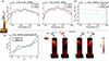 |
Fig. 3 Schematic of the excitation that enables extrinsic chirality in Sample C-Au (a) Sample C-Au is excited with LCP or RCP, at ±20° oblique incidence, and the difference between the NW signal and the substrate is measured at 1225 Hz. (b) Difference of the PAS signal for LCP and RCP excitation for the incidence angles −20°, 0° and 20°. (c) Experimental normalized absorption difference as a function of the incidence angle, at 720 nm and 800 nm. (d) Distribution of the absorption density in a single NW on the substrate, excited with LCP and RCP, at 720 nm and at ±20° of incidence. LCP leads to stronger absorption in the Au sidewalls than RCP for +20°, which inverts at −20°, in agreement with the PAS experiment. |
Besides precise microscope positioning and beam-waist tuning on the nanostructured areas [26], the novelty of our set-up lies in parallel chopper frequency and incident power tuning. Namely, with nanostructures on thermally insulating substrates (such as commercial soda-lime glass), PAS is highly sensitive to the nanomaterial on the top, as the nanostructure absorption creates the heat wave which stays confined to the top. In this case, even with powers on the order of mW and at lower frequencies (f = 81 Hz), we were able to characterize absorption and extrinsic chirality in 20–50 nm of absorbing material [27]. However, with substrates that are thermally conductive and absorbing, the heat sinks into the substrate, leading to the lower nanostructure signal hidden by the substrate response. This can be partially solved by increasing f; however, the PAS amplitude decreases with the f increase, thus deteriorating signal to noise ratio. Finally, the increase of the incident power at higher modulation frequencies can be used to improve PAS sensitivity while discriminating the nanostructure response from the background substrate. All the PAS signals presented here are normalized to the incident power at that frequency. Moreover, we anticipate that investigating both PAS amplitude and phase while continuously tuning the frequency, and, in parallel, spectrally investigating the resonances, could reveal the depth sensitivity, and lead to novel applications in heat transport at the nanoscale.
4 Conclusion
We have studied semiconductor and semiconductor-plasmonic NW ensembles by means of photo-acoustic technique with modulation frequency in kHz range, and the laser light source in the near-infrared range. In semiconductor NW sample, the increase of the chopper frequency from 54 Hz to 1225 Hz leads to the more precise discrimination of the resonant leaky-waveguide mode peaking at 780 nm, in great agreement with numerical predictions. At 1225 Hz, the same sample, asymmetrically covered by Au, has hybridized plasmonic-photonic mode, broadened and red-shifted to ~850 nm. Furthermore, with this modulation frequency we were able to detect weak extrinsic chiral behavior arising from the asymmetric geometry of Au on the NW sidewalls. We believe that tunable modulation frequency will become an important parameter for both revealing of the depth sensitivity, and for accessing novel photo-thermal phenomena at the nanoscale. Furthermore, enriching the set-up with photo-elastic modulators could allow for improved sensitivity of chiral sensing at much higher modulation frequencies, thus discriminating the properties of thin surface layers of samples [18].
Funding
This research received no external funding.
Conflicts of interest
The authors have nothing to disclose.
Data availability statement
Data obtained in this work are not publicly available at this time but may be obtained from the authors upon reasonable request.
Author contribution statement
Conceptualization, N.B., E.P. and A.B.; Methodology, E.P.; Sample Fabrication, T.H.; Software, C.Sk. and A.B.; Validation, C.S., G.L., R.L.V. and A.B.; Formal Analysis, J.S.-L. and E.P.; Investigation, N.B.,J.S.-L, and C.Sk.; Data Curation, E.P.; Writing – Original Draft Preparation, N.B. and E.P.; Writing – Review & Editing, all authors; Visualization, E.P.; Supervision, E.P. and A.B.
Acknowledgments
The authors thank the ENSEMBLE3 Project carried within the Teaming for Excellence Horizon 2020 program of the European Commission (GA No. 857543). A.B. and E.P. acknowledges LASAFEM Sapienza Università di Roma Infrastructure Project 2017 n. MA31715C8215A268 and PRIN 2022 PNRR Project INSPIRE n. P2022LETN5 founded by the European Union – NextGenerationEU. C. Skubisz acknowledges PNRR MUR project PE0000023-NQSTI. All authors acknowledge M. Magi for technical support.
References
- Wang J-J, Fu C, Cheng H-Y, Tong X-W, Zhang Z-X, Wu D, Chen L-M, Liang F-X, Luo L-B, Leaky mode resonance-induced sensitive ultraviolet photodetector composed of graphene/small diameter silicon nanowire array heterojunctions, ACS Nano 15(10), 16729–16737 (2021). https://doi.org/10.1021/acsnano.1c06705. [Google Scholar]
- Zhang, C., Hu, H., Ma, C. et al. Quantum plasmonics pushes chiral sensing limit to single molecules: a paradigm for chiral biodetections, Nat. Commun. 15, 2 (2024). https://doi.org/10.1038/s41467-023-42719-z. [Google Scholar]
- Bychto L, Maliński M. Determination of the optical absorption coefficient spectra of thin semiconductor layers from their photoacoustic spectra. Int. J. Thermophys. 39, 103 (2018). https://doi.org/10.1007/s10765-018-2424-x. [Google Scholar]
- Park T, Kim J, Ko R, Yoo H, Light in, sound keys out: photoacoustic PUFs from stochastic nanocomposites, Nat. Commun. 16, 7323 (2025). https://doi.org/10.1038/s41467-025-62747-1. [Google Scholar]
- Djordjević KL, Markushev DK, Popović MN, Nesić MV, Galović SP, Lukić DV, Markushev DD, Photoacoustic characterization of TiO2 thin-films deposited on silicon substrate using neural networks. Materials 16(7), 2865 (2023). https://doi.org/10.3390/ma16072865. [Google Scholar]
- Petronijevic E, Leahu G, Mussi V, Sibilia C, Bovino AF, Photoacoustic technique for the characterization of plasmonic properties of 2D periodic arrays of gold nanoholes, AIP Adv. 7(2), 025210 (2017). https://doi.org/10.1063/1.4977545. [Google Scholar]
- Zelewski SJ, Zhou Z, Li F, Kang X, Meng Y, Ho JC, Kudrawiec R. Optical Properties of In2xGa2-2xO3 Nanowires Revealed by Photoacoustic Spectroscopy, ACS Appl. Mater. Interfaces, 11(21), 19260–19266, 2019. https://doi.org/10.1021/acsami.9b00756. [Google Scholar]
- Leahu G, Petronijevic E, Belardini A, Centini M, Li Voti R, Hakkarainen T, Koivusalo E, Guina M, Sibilia C, Photo-acoustic spectroscopy revealing resonant absorption of self-assembled GaAs-based nanowires, Sci. Rep. 7(1), 2833 (2017). https://doi.org/10.1038/s41598-017-02839-1. [Google Scholar]
- Petronijevic E, Leahu G, Skubisz C, Li Voti R, Sibilia C, Belardini A, Listening to nanostructures' absorption with many degrees of freedom: widely tunable photo-acoustic characterization, Eur. Phys. J. Plus 140-613 (2025). https://doi.org/10.1140/epjp/s13360-025-06578-5. [Google Scholar]
- Hakkarainen, TV, Schramm A, Mäkelä J, Laukkanen P, Guina M. Lithography-free oxide patterns as templates for self-catalyzed growth of highly uniform GaAs nanowires on Si(111), Nanotechnology 26, 275301 (2015). https://doi.org/10.1088/0957-4484/26/27/275301. [Google Scholar]
- Petronijevic E, Belardini A, Leahu G, Hakkarainen T, Rizzo Piton M, Koivusalo E, Sibilia C, Broadband optical spin dependent reflection in self-assembled GaAs-based nanowires asymmetrically hybridized with Au, Sci. Rep. 11, 4316 (2021). https://doi.org/10.1038/s41598-021-83899-2. [Google Scholar]
- Lumerical Solutions, Inc. http://www.lumerical.com/tcadproducts/fdtd/. [Google Scholar]
- Papatryfonos K, Angelova T, Brimont A, Reid B, Guldin S, Smith PR, Tang M, Li K, Seeds AJ, Liu H, Selviah DR, Refractive indices of MBE-grown AlxGa1-xAs ternary alloys in the transparent wavelength region, AIP Adv. 11, 025327 (2021). https://doi.org/10.1063/5.0039631. [Google Scholar]
- Petronijevic E, Leahu G, Belardini A, Centini M, Li Voti R, Hakkarainen T, Koivusalo E, Guina M, Sibilia C, Resonant absorption in GaAs-based nanowires by means of photo-acoustic spectroscopy, Int. J. Thermophys. 39, 45 (2018). https://doi.org/10.1007/s10765-018-2365-4. [Google Scholar]
- Chen Y, Anttu N, Sivakumar S, Gompou E, Magnusson MH, Optical far-field extinction of a single GaAs nanowire towards in situ size control of aerotaxy nanowire growth, Nanotechnology 31, 134001 (2020). https://doi.org/10.1088/1361-6528/ab5fe4. [Google Scholar]
- Becucci M, Bracciali M, Ghini G, Lofrumento C, Pietraperzia G, Ricci M, Tognaccini L, Trigari S, Gellini C, Feis A, Silver nanowires as infrared-active materials for surface-enhanced Raman scattering, Nanoscale 10, 9329-9337 (2018). https://doi.org/10.1039/C8NR00537K. [Google Scholar]
- Benedetti A, Alam B, Esposito M, Tasco V, Leahu G, Belardini A, Li Voti R, Passaseo A, Sibilia C, Precise detection of circular dichroism in a cluster of nano-helices by photoacoustic measurements, Sci. Rep. 7, 5257 (2017). https://doi.org/10.1038/s41598-017-05193-4. [Google Scholar]
- Spaeth P, Adhikari S, Dieter Baaske M, Pud S, Ton J, Orrit M, Photothermal circular dichroism of single nanoparticles rejecting linear dichroism by dual modulation, ACS Nano 15(10), 16277–16285 (2021). https://doi.org/10.1021/acsnano.1c05374. [CrossRef] [Google Scholar]
- Kuroda R, Harada T, Shindo Y, A solid-state dedicated circular dichroism spectrophotometer: Development and application, Rev. Sci. Instrum. 72, 3802–3810 (2001). https://doi.org/10.1063/1.1400157. [Google Scholar]
- Arteaga O, Sancho-Parramon J, Nichols S, Maoz B.M, Canillas A, Bosch S, Markovich G, Kahr B, Relation between 2D/3D chirality and the appearance of chiroptical effects in real nanostructures, Opt. Express 24, 3, 2242 (2016). https://doi.org/10.1364/OE.24.002242. [Google Scholar]
- Zubritskaya I, Maccaferri N, Ezeiza X.I, Vavassori P, Dmitriev A, Magnetic control of the chiroptical plasmonic surfaces, Nano Lett. 18, 302−307 (2018). https://doi.org/10.1021/acs.nanolett.7b04139. [Google Scholar]
- Petrucci G, Gabbani A, Faniayeu I, Pedrueza-Villalmanzo E, Cucinotta G, Atzori M, Dmitriev A, Pineider F, Macroscopic magneto-chiroptical metasurfaces, Appl. Phys. Lett. 118, 251108 (2021). https://doi.org/10.1063/5.0050797. [Google Scholar]
- Leahu G, Petronijevic E, Belardini A, Centini M, Sibilia C, Hakkarainen T, Koivusalo E, Rizzo Piton M, Suomalainen S, Guina M, Evidence of optical circular dichroism in GaAs-Based nanowires partially covered with gold, Adv. Opt. Mater. 5(16), 1601063 (2017). https://doi.org/10.1002/adom.201601063. [Google Scholar]
- Hakkarainen T, Petronijevic E, Rizzo Piton M, Sibilia C, Demonstration of extrinsic chirality of photoluminescence with semiconductor-metal hybrid nanowires, Sci. Rep. 9, 5040 (2019). https://doi.org/10.1038/s41598-019-41615-1. [Google Scholar]
- Belardini A, Leahu G, Petronijevic E, Hakkarainen T, Koivusalo E, Rizzo Piton M, Talmila S, Guina M, and Sibilia C, Circular dichroism in the second harmonic field evidenced by asymmetric Au coated GaAs nanowires, Micromachines 11, 225 (2020). https://doi.org/10.3390/mi11020225. [Google Scholar]
- Petronijevic E, Ali H, Freddi S, Anzi L, Sordan R, Bollani M, Andreani LC, Belardini A, Photo-acoustic spectroscopy detects nanostructures against resonant and absorbing substrates, J. Eur. Opt. Society-Rapid Publ. 21, 49 (2025). https://doi.org/10.1051/jeos/2025048. [Google Scholar]
- Skubisz C, Petronijevic E, Leahu G, Cesca T, Scian C, Mattei G, Sibilia C, Belardini A. Photo-acoustic technique with widely tuneable laser: metasurface circular dichroism response, J. Eur. Opt. Society-Rapid Publ. 20, 1 (2024). https://doi.org/10.1051/jeos/2024016. [Google Scholar]
All Figures
|
Fig. 1 (a) Photo-acoustic spectroscopy, allows for tunable polarization, power, modulation frequency, incidence angle; inset: schematic of the two samples. Both have diameter of 165 nm and height of 4.6 μm; Sample C-Au has two out of six sidewalls covered by 20 nm Au. (b) Simulation of a single NW of Sample C, in the air and standing on the Si substrate, and the 3D distribution of the absorption density at the resonance of 780 nm. The Si substrate widens the leaky waveguide mode resonance. (c) Simulation of a single NW covered by Au, and the 3D distribution of the absorption density at 850 nm. Here, the substrate strongly influences absorption as its parts contain absorbing material. |
| In the text | |
|
Fig. 2 (a) PAS signal amplitude of samples C, C-Au and the substrate (without Au), excited at normal incidence and modulated with 54Hz, 408 Hz and 625 Hz chopper frequency; the excitation is at normal incidence with linear polarization. All the signals are normalized to the incident laser power at the corresponding wavelength. (b) Normalized PAS signal for both nanostructured samples is obtained by subtracting the substrate signal from the NW signal, and normalizing each spectra to its maximum. The resonant modes appear at higher frequencies, and their bandwidth shrinks. (c) PAS difference between the NWs and the substrate for Sample C and Sample C-Au agree with the NW modes predicted by simulations. |
| In the text | |
|
Fig. 3 Schematic of the excitation that enables extrinsic chirality in Sample C-Au (a) Sample C-Au is excited with LCP or RCP, at ±20° oblique incidence, and the difference between the NW signal and the substrate is measured at 1225 Hz. (b) Difference of the PAS signal for LCP and RCP excitation for the incidence angles −20°, 0° and 20°. (c) Experimental normalized absorption difference as a function of the incidence angle, at 720 nm and 800 nm. (d) Distribution of the absorption density in a single NW on the substrate, excited with LCP and RCP, at 720 nm and at ±20° of incidence. LCP leads to stronger absorption in the Au sidewalls than RCP for +20°, which inverts at −20°, in agreement with the PAS experiment. |
| In the text | |
Current usage metrics show cumulative count of Article Views (full-text article views including HTML views, PDF and ePub downloads, according to the available data) and Abstracts Views on Vision4Press platform.
Data correspond to usage on the plateform after 2015. The current usage metrics is available 48-96 hours after online publication and is updated daily on week days.
Initial download of the metrics may take a while.