| Issue |
J. Eur. Opt. Society-Rapid Publ.
Volume 22, Number 1, 2026
Nano-optoelectronics: from novel materials and nanostructures to innovative applications
|
|
|---|---|---|
| Article Number | 38 | |
| Number of page(s) | 5 | |
| DOI | https://doi.org/10.1051/jeos/2026031 | |
| Published online | 12 May 2026 | |
Short Communication
Indoor energy harvesting enhancement: Pb-free perovskite solar cell with nanograting contact
1
GDAF-UC3M, Displays and Photonics Applications Group, Universidad Carlos III de Madrid, Spain
2
INAM-UJI, Institute of Advanced Materials, Universitat Jaume I de Castellón, Spain
3
Instituto de Micro y Nanotecnología IMN-CNM, CSIC, CEI UAM+CSIC, Spain
* Corresponding author: This email address is being protected from spambots. You need JavaScript enabled to view it.
Received:
19
December
2025
Accepted:
22
March
2026
Abstract
Halide perovskite materials have spread in solar cells and photodetectors because of their excellent possibilities for tuning their absorption wavelengths, ease of fabrication, and low carbon footprint. However, their main drawbacks are related to their short device lifetime and stability problems in addition to limited efficiency at certain wavelength. For this reason, in this letter, we design a metasurface that can be integrated into a particularly long-life, stable, and sustainable perovskite solar cell with the aim of enhancing its performance under indoor conditions. The metasurface has been designed and numerically simulated to enhance the halide perovskite response at the typical emission wavelengths of indoor LEDs. Adjusting the response of these solar cells to those specific spectral ranges by metasurfaces may create novel energy harvesting devices.
Key words: Perovskite solar cell / Nanostructured grating / Indoor energy harvesting / Pb-free / FDTD methods
© The Author(s), published by EDP Sciences, 2026
 This is an Open Access article distributed under the terms of the Creative Commons Attribution License (https://creativecommons.org/licenses/by/4.0), which permits unrestricted use, distribution, and reproduction in any medium, provided the original work is properly cited.
1 Introduction
Halide perovskite solar cells (PSCs) are revolutionizing solar energy conversion due to their low-cost fabrication, high efficiencies (single-junction reach 26.7%, and tandem exceed 34%) [1, 2], and versatility for diverse applications including IoT and building integration [3, 4]. Their inherent properties, such as faster carrier dynamics and tunable bandgaps, are key to achieving up to 57% theoretical efficiency under indoor illumination, significantly exceeding the outdoor Shockley-Queisser limit of ∼34% [5, 6]. However, PSCs struggle with long-term stability due to crystallization defects, moisture, oxygen, and ionic migration [7]. Research currently focuses on developing stable, durable, and sustainable (Pb-free) materials and architectures to reach full deployment potential [8–13]. One crucial strategy for enhancement is the incorporation of nanophotonic elements like metasurfaces [14]. These structures effectively manipulate light propagation to boost absorption at relevant wavelengths, increasing photocurrent, and enable functionalities such as color tunability and enhanced light trapping [15–17]. Nanograting structures are particularly promising for improved light management [18]. They introduce periodic patterns to increase light trapping and extend the optical path, which is crucial for thin-film devices where light absorption is limited by layer thickness. This approach may either minimize Pb content or increase absorption in defective Sn-based PSCs. Optimized gratings support guided modes and resonances, increasing PCE without adding fabrication complexity [19]. Since poor positioning or refractive index mismatch can compromise performance [20], this study focuses on the numerical design of an optimal nanograting metasurface. Our goal is to improve the indoor performance of a Pb-free INAM-UJI PSC [21] by engineering a 1D diffraction grating within the hole transport layer (HTL) to increase absorbance at characteristic LED illumination peaks.
2 Methodology
Numerical simulations were performed using the finite-difference time-domain (FDTD) method (Lumerical, Ansys©). The unit cell reproduces the optically significant structure of the PSC shown in Figure 1a. Based on devices characterized in Ref. [21], the cell comprises a 200 nm active layer of FASI (FASnI3) modified with an OM6 organic additive to enhance stability. This layer is sandwiched between carrier extraction layers: a 30 nm hole transport layer (HTL) of PEDOT:PSS and a 30 nm electron transport layer (ETL) of C60. A 250 nm indium tin oxide (ITO) anode and a 100 nm silver cathode serve as contacts, with a negligible BCP (bathocuproine) buffer layer and SiO2 encapsulation. As it is established in [22] the optical properties for PEDOT are essentially constant. The rest of the optical parameters used as inputs come from both literature and manufacturers, including the ones of the original planar device [21]. Periodic boundary conditions (PBC) were applied along the x- and y-axes, with perfectly matched layers (PML) in the z-axis to simulate propagation. The device was illuminated by a plane wave (z-propagating, x-polarized) with a spectrum derived from the average of experimental indoor LED measurements taken at Carlos III University of Madrid, as shown in Figure 1b.
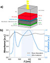 |
Figure 1 (a) The planar structure of the perovskite solar cell that has been used in this work, including the most significant layers. In particular, an OM6-modified FASI is used as active layer with the aim of enhancing stability. (b) Spectral profile of the absorbance of the considered planar perovskite solar cell (left-axis) and the spectral emission of typical LED of indoor lighting systems (right axis). |
The absorbed optical power in the halide perovskite layer was calculated using electric field intensity (|E|2) and dielectric permittivity (ϵ) data obtained from 3D FDTD monitors, same size as the perovskite active layer. The absorbed power density is defined as: (1)where ω is the angular frequency of incident radiation and Im(ϵ) is the imaginary part of the perovskite dielectric constant. Total absorption was determined by integrating this optical power over the simulation volume. Figure 1b compares the Sn-OM6 cell absorption with the average conventional LED lighting emission spectrum. While the cell exhibits a broad absorption band centered at 460 nm, absorption decreases significantly in the higher wavelength region, highlighting a clear opportunity for optimization.
3 Results and discussion
We focus on the application of these devices in energy harvesting for indoor conditions. Therefore, we have studied the most widely distributed luminaires: LEDs. LED lighting implies a very different illumination from the usual solar spectrum. While the first reaches a standard of 100 mW cm−2 (at AM1.5G), indoor lighting only reaches a small fraction of it. Indeed, the spectrum is very different, with a usual peak around 450 nm due to the blue LED inside, and a spread emission band around 600 nm due to the phosphor inside the encapsulated luminaire. White LEDs can achieve combinations of desired ambient lighting (cool or warm lights) by balancing both emissions. To get a good overview of real situations in which future applications will be developed, we have measured a set of scenarios in actual classrooms and laboratories of Carlos III University of Madrid (UC3M), discarding those measurements close to the windows during daylight hours (where the outdoor lighting is at least one order of magnitude higher than the indoor one). As was commented on, Figure 1b depicts the average emission spectrum of the received light on horizontal planes at user heights in those scenarios (meanly, working tables or experimental setups).
After a prospective numerical work, the proposed nanostructured grating is finally introduced in the HTL layer (see Fig. 2) composed of ordered stripes with a certain width in x-axis and a length exceeding the unit cell size along y-axis to simulate an infinite bar. Thus, the main geometric parameters of this structure are the height (h) and width (w) of the grating, which are optimized to maximize the absorption of the active layer at the dominant wavelengths of indoor LEDs, as shown in Figure 1b. Furthermore, the size of the unit cell (p) and the remaining thickness of the planar section of the HTL (hPEDOT:PSS) are also included. For the discretization, auto non-uniform mesh (mesh accuracy 4) was selected. To improve the convergence of the results, a refinement mesh in the grating was used with a 5 nm size along the x-, y- and z-axis.
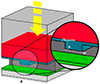 |
Figure 2 Scheme of the proposed nanograting in the HTL surface to provide a larger light path control and enhance the effective absorbance of the PSC. Inset: detail of the structure with the most significant geometrical parameters. |
We parametrically investigated the nanograting’s geometrical characteristics (like shape and size) to find the optimal design for enhancing light absorption within specific spectral ranges. To do this, we defined an application-oriented absorption efficiency that specifically weights the absorption of the cell by the actual measured indoor LED light spectrum (as shown in Fig. 1b). This weighting, formalized in equation (2), ensures that the calculated efficiency reflects the true performance of the device in indoor real-world conditions. (2)
(2)
Quantification of this absorption enhancement is accomplished through the introduction of a Figure of Merit (FOM) formally defined as the differential absorption efficiency (in percentage) as shown in equation (3): (3)
(3)
Being η and η0 the absorption efficiency with and without the integration of the nanograting structure, respectively.
Figure 3 shows a 3D plot of the percentage differential absorption efficiency versus the geometric dimensions of the structure. To facilitate the concise presentation and clarification of the data, the derived results are graphically represented as a function of the following geometric parameters: the aspect ratio of the stripes, defined as the height-width ratio and the period of the modeled unit cell (see Fig. 2). The plot demonstrates a continuous consistent response, showing that the magnitude of the defined FOM-the differential absorption efficiency-is positively correlated with the increasing period in the studied interval (100 nm–200 nm) except for a short range close to 200 nm at low aspect ratio, while it first increases, and then decreases with decreasing ratio. A peak value of 7.09 percentage points constitutes the maximum observed, in a ratio of h/w = 0.7 and a period of 190 nm. This optimum case, highlighted in the Figure 3, particularly considers w = 100 nm, being the width for which the best result has been achieved. Moreover, it is worth mentioning that this result is specific to the active layer, indicating a potential similar improvement in the generated photocurrent.
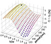 |
Figure 3 Differential absorption efficiency of the nanograting PSC as a function of both the ratio height/width of the stripes and the unit cell size or period. The width of the stripes has been fixed to a value of w = 100 nm. The maximum (91.14%) is shown at 190 nm period and a ratio of 0.7, represented against the reference (84.05%). |
The active layer absorbance spectrum for both the planar reference structure and the proposed nanograting structure integrated into the HTL is shown in Figure 4. Near-field profiles obtained resolve a field redistribution around the nanograting that increases the light intensity in the active layer, and thus, absorption. The nanograting primarily improves the overall absorbance for incident wavelengths (λ) less than 675 nm, although it causes a degradation in performance for λ > 675 nm. Crucially, the performance of the PSC is significantly improved within the specific spectral region of interest under LED illumination, particularly due to a pronounced increase in the absorption in the active layer within the λ interval of 520 nm to 620 nm. This region directly aligns with a major LED emission peak at ∼600 nm. Although x-polarized light shows a better response, y-polarized one also slightly enhances the planar case around similar wavelength intervals, with an increment of 4.59 percentage points. Thus, whenever the cell is under indoor illumination, the absorption will be improved, also showing polarization sensitivity. This enhancement is characterized by a blue-shift in the peak absorbance from ∼650 nm in the planar structure to ∼615 nm in the nanostructure, achieving a closer spectral match to the ∼600 nm LED peak irradiance. Furthermore, the proposed PSC exhibits a slight but beneficial increase in absorbance in the spectral region corresponding to the secondary LED emission peak (∼450 nm), which also significantly increases overall performance in that region. Thus, this nanostructure effectively enhances the overall absorbance in the spectral range from 400 nm to 650 nm, relative to the planar structure, while absorption decreases for λ > 650 nm, signifying the successful achievement of spectral shape matching between the active layer absorbance profile and the LED irradiance spectrum within the critical operating interval. Other 2D structures have been tested, but as their results are close to the ones exposed here, significant limitations due to their difficult nanofabrication and integration into device architectures may reduce the feasibility of using them to improve these PSCs for indoor applications.
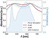 |
Figure 4 Active layer absorbance for the planar and optimized structures is presented as a function of incident wavelength (λ). The characterized LED emission spectrum is superimposed to assess the resulting performance enhancement under the specified illumination. |
4 Conclusion
In this work, we first established a magnitude of interest that allows us to pinpoint the performance enhancement of a novel Pb-free Sn-based perovskite solar cell in an indoor room. We weigh the spectral absorbance of the cell by an irradiance spectrum, which is the average of a weighed efficiency, which is dependent on the lighting conditions around the cell. This leads to a simple figure of merit to understand the level of theoretical enhancement, by comparing the planar cell efficiency, taken as the reference case, with that of the cell with the proposed nanograting, as the improved one. To isolate the optical impact of the nanostructure, our model assumes constant electrical parameters, acknowledging that the electronic challenges of increased interfacial area are effectively addressed in experimental settings via surface passivation layers. Moreover, such nanogratings can facilitate improved carrier extraction by reducing the transport distance to the contacts, provided that conformal film deposition is achieved.
We have explored several geometries, achieving the best results with the use of 1D grating simulated in the device structure that was manufactured in one of our previous works. An optimized result is obtained at a geometrical form factor of the grid of h/w = 0.7 and a period of 190 nm. An average of 5.84% optical enhancement (with a maximum of 7.09% under x-polarization) confirms the feasibility of using nanograting-based Pb-free cells for indoor energy harvesting. In line with literature [23], our results suggest a proportional boost in electron-hole generation and short-circuit current, provided carrier extraction remains efficient. These results allow exploring Internet of Things applications where these cells can be used as energy harvesting photovoltaic devices, recycling ambient light to create fully autonomous wireless (but cloud-connected) systems.
Funding
This research was funded by Research Projects STEP-UP (TED2021-131600B-C31 and TED2021-131600B-C33), PLEDs (PID2022-140090OB-C21 and PID2022-140090OB-C22) and HyQuaNa (PID2022-137857NA-I00), financed by the Spanish Ministry of Science and Innovation MCIN/AEI/10.13039-/501100011033, STEP-UP also by the European Union “NextGenerationEU”/PRTR”, and PLEDs by “ERDF A way of making Europe”.
Conflicts of interest
The authors have nothing to disclose.
Data availability statement
There is an associated dataset available at: https://doi.org/10.21950/J69M96.
Author contribution statement
Conceptualization, B.G-C, A.B., I.M., R.V., and A.G-M; Methodology, R.V., B.G-C, A.B., E.L-F and D.S.; Software, D.S.; Validation, Formal Analysis, Investigation and Resources: all authors; Data Curation, D.S., R.V.; Writing – Original Draft Preparation, R.V., B.G-C and D.S; Writing – Review Editing, Visualization, all authors; Supervision, Project Administration, Funding Acquisition, R.V.
Acknowledgments
A.B. thanks MICINN for the Ramon y Cajal Fellowship (grant No. RYC2021-030880-I).
References
- Green MA, Dunlop ED, Yoshita M, et al., Solar cell efficiency tables (version 66), Prog. Photovolt. Res. Appl. 33, 795–810 (2025). [Google Scholar]
- LONGi, Is M6 wafer silicon-perovskite tandem cells new efficiency record?, (2025). [Google Scholar]
- Tiwari, JP Flexible perovskite solar cells: A futuristic IoTs powering solar cell technology, Small Methods. 9, e2400624 (2025). [Google Scholar]
- Chen W, Mularso KT, Jo B, Jung HS, Indoor light energy harvesting perovskite solar cells: from device physics to AI-driven strategies, Mater. Horiz. 12(11), 3691–3711 (2025). [Google Scholar]
- Qamar MZ, Khalid Z, Shahid R, et al., Advancement in indoor energy harvesting through flexible perovskite photovoltaics for self-powered IoT applications, Nano Energy. 129, 109994 (2024). [Google Scholar]
- Chai Z, Lin H, Bai H, et al., Application of metal halide perovskite in internet of things, Micromachines. 15, 1152 (2024). [Google Scholar]
- Zhang H, Fu X, Tang Y, et al., Phase segregation due to ion migration in all-inorganic mixed halide perovskite nanocrystals, Nat. Commun. 10, 1088 (2019). [Google Scholar]
- López-Fernández, I; Valli, D; Wang, CY, et al., Lead-free halide perovskite materials and optoelectronic devices: Progress and prospective. Adv. Funct. Mater. 34, 6, 2307896 (2023). [Google Scholar]
- Ahmed S, Gondal MA, Alzahrani AS, et al., Recent trends and challenges in lead-free perovskite solar cells: A critical review. ACS Appl. Energy Mater. 7(4), 1382–1397 (2024). [Google Scholar]
- Miah, MH, Khandaker, MU, et al., Lead-free alternatives and toxicity mitigation strategies for sustainable perovskite solar cells: a critical review. Mater. Adv. 6, 2718–2752 (2025). [Google Scholar]
- Diguna, LJ, Lim, A, Firdaus, Y, et al., The role of perovskite composition, dimensionality, and additives in lead-free perovskite solar cell longevity: A review. Sustain. Energy Fuels. 9, 6413–6438 (2025). [Google Scholar]
- Shah AUI, Meyer EL, Perovskite-based solar cells in photovoltaics for commercial scalability: Current progress, challenges, mitigations and future prospectus, Sol. Energy. 2868, 113172 (2025). [Google Scholar]
- Ali KM, Mohsen AA, Allam NK. Lead-free perovskite materials for optoelectronic and solar energy applications. Solar Energy Mater. Solar Cells 295, 114025 (2026). [Google Scholar]
- Cheng P, An Y, Jen AK, Lei D, New nanophotonics approaches for enhancing the efficiency and stability of perovskite solar cells, Adv. Mater. 36, 2309459 (2024). [Google Scholar]
- Almeida E, Alexandre M, Santos IM, et al., Photonic-enhanced perovskite solar cells: Tailoring color and light capture, ACS Omega. 9, 42839–42849 (2024). [Google Scholar]
- Delgado-Rodríguez S, Jaldo Serrano E, Elshorbagy MH, et al., Spectral control by silver nanoparticle-based metasurfaces for mitigation of UV degradation in perovskite solar cells, Nanomaterials. 14, 1582 (2024). [Google Scholar]
- Ying Z, Guo X, Du H, et al., Hierarchical micro/nanostructured perovskite/silicon tandem solar cells with fully textured solution-processed conformal perovskite absorbers, ACS Energy Lett. 9, 4018–4023 (2024). [Google Scholar]
- Gu X, Li Z, Rusli E, et al., An optical study on the enhanced light trapping performance of the perovskite solar cell using nanocone structure, Sci. Rep. 14, 13363 (2024). [Google Scholar]
- Feng J, Wang X, Li J, et al., Resonant perovskite solar cells with extended band edge, Nat. Commun. 14, 5392 (2023). [Google Scholar]
- Harwell J, Burch J, Fikouras A, et al., Patterning multicolor hybrid perovskite films via top-down lithography, ACS Nano. 13, 3823–3829 (2019). [Google Scholar]
- Galve-Lahoz S, Sánchez-Diaz J, Echeverría-Arrondo C, et al., Addressing ambient stability challenges in pure FASnI3 perovskite solar cells through organic additive engineering, J. Mater. Chem. A. 12, 21933–21943 (2024). [Google Scholar]
- Chen, CW, Hsiao, S-Y., Chen, S-Y, et al., Optical properties of organometal halide perovskite thin films and general device structure design rules for perovskite single and tandem solar cells. J. Mater. Chem. A. 3, 9152–9159 (2015) [Google Scholar]
- Hu, Z, García-Martín, JM, Li, Y, Billot, L., Sun, B, Fresno, F, García-Martín, A, González, MU, Aigouy, L, Chen, Z TiO2 nanocolumn arrays for more efficient and stable perovskite solar cells, ACS Appl. Mater. Interfaces. 12(5), 5979–5989 (2020). [Google Scholar]
All Figures
|
Figure 1 (a) The planar structure of the perovskite solar cell that has been used in this work, including the most significant layers. In particular, an OM6-modified FASI is used as active layer with the aim of enhancing stability. (b) Spectral profile of the absorbance of the considered planar perovskite solar cell (left-axis) and the spectral emission of typical LED of indoor lighting systems (right axis). |
| In the text | |
|
Figure 2 Scheme of the proposed nanograting in the HTL surface to provide a larger light path control and enhance the effective absorbance of the PSC. Inset: detail of the structure with the most significant geometrical parameters. |
| In the text | |
|
Figure 3 Differential absorption efficiency of the nanograting PSC as a function of both the ratio height/width of the stripes and the unit cell size or period. The width of the stripes has been fixed to a value of w = 100 nm. The maximum (91.14%) is shown at 190 nm period and a ratio of 0.7, represented against the reference (84.05%). |
| In the text | |
|
Figure 4 Active layer absorbance for the planar and optimized structures is presented as a function of incident wavelength (λ). The characterized LED emission spectrum is superimposed to assess the resulting performance enhancement under the specified illumination. |
| In the text | |
Current usage metrics show cumulative count of Article Views (full-text article views including HTML views, PDF and ePub downloads, according to the available data) and Abstracts Views on Vision4Press platform.
Data correspond to usage on the plateform after 2015. The current usage metrics is available 48-96 hours after online publication and is updated daily on week days.
Initial download of the metrics may take a while.