| Issue |
J. Eur. Opt. Society-Rapid Publ.
Volume 22, Number 1, 2026
Recent Advances on Optics and Photonics 2026
|
|
|---|---|---|
| Article Number | 16 | |
| Number of page(s) | 16 | |
| DOI | https://doi.org/10.1051/jeos/2026013 | |
| Published online | 20 March 2026 | |
Research Article
Design of Si3N4-TFLN heterogeneous integrated device with phase modulation and frequency doubling: Performance optimization and application prospects
Army Engineering University Shijiazhuang Campus, Shijiazhuang 050003, China
* Corresponding author: This email address is being protected from spambots. You need JavaScript enabled to view it.
Received:
9
January
2026
Accepted:
14
February
2026
Abstract
Electro-optic phase modulation is a core technology for signal processing in optical communication and microwave photonics, yet the current multifunctional integrated devices for high-bandwidth phase modulation and efficient frequency doubling suffer from critical bottlenecks including large crosstalk, excessive chip area, bandwidth-voltage trade-off, and single material performance limitations. To address these issues, this study proposes a Si3N4-TFLN heterogeneous integrated design scheme by synergizing the low-loss property of silicon nitride and the strong electro-optic effect of thin-film lithium niobate. A Dual-Drive Mach-Zehnder Modulator (DD-MZM) and a racetrack Micro-Ring Resonator (MRR) with high quality-factor and large Free Spectral Range (FSR) are cascaded to realize the monolithic integration of high-precision phase modulation and microwave signal frequency doubling. Co-simulation results show that the designed device achieves an electro-optic modulation bandwidth of 72 GHz and a half-wave voltage-length product of 2.8 V · cm, which well reconciles the bandwidth-voltage trade-off. The device exhibits a frequency-doubling efficiency of 15%, 30.4% higher than that of the single TFLN-based MRR. The cascaded coupling structure suppresses the functional crosstalk to −38 dB, and the total chip layout area is only 3.648 mm2, over 60% smaller than that of the existing similar devices. This work provides a high-performance on-chip solution for high-density integrated systems in optical communication, microwave photonics, and quantum information processing.
Key words: Dual-drive Mach-Zehnder modulator (DD-MZM) / Frequency doubling / Lithium niobate (LN) / Micro-ring resonator (MRR) / Phase modulation / Frequency doubling
© The Author(s), published by EDP Sciences, 2026
 This is an Open Access article distributed under the terms of the Creative Commons Attribution License (https://creativecommons.org/licenses/by/4.0), which permits unrestricted use, distribution, and reproduction in any medium, provided the original work is properly cited.
1 Introduction
For application scenarios such as optical communications [1–3], fiber-optic sensing [4, 5], and microwave photonics [6–9], the efficiency and precision of electro-optic phase modulation technologies have become key drivers for advancing system performance. Silicon-based electro-optic phase modulators [10, 11], leveraging their compatibility with semiconductor processes, low power consumption, and high integration potential, have emerged as a promising technology in the field of short-range optical interconnections. However, constrained by intrinsic material properties such as low electro-optic coefficients and high losses, silicon-based devices still face bottlenecks in ultra-high-speed, long-distance, or high-power scenarios. In contrast, lithium niobate (LN) phase modulators, with their comprehensive advantages including exceptional frequency bandwidth, fast response speed, low insertion loss, high signal-to-noise ratio, low half-wave voltage, and excellent stability, have become the core device for realizing electro-optical conversion, demonstrating great potential for system integration and broad application prospects [12, 13].
However, the high-frequency response of traditional bulk LN modulators is affected by factors such as “microwave optical field velocity matching” and “electrode parasitic parameters,” resulting in limited electro-optic bandwidth [14]. The inherent size and integration bottlenecks [15, 16] of bulk LN modulators impede seamless integration with mainstream silicon-based photonic platforms, consequently restricting their deployment in high-density integrated systems.
To overcome this limitation, thin-film technology has become the core direction for the development of LN devices. Internationally, TFLN technology has made groundbreaking progress. The research team from the University of California, Santa Barbara developed a TFLN modulator with a bandwidth of over 100 GHz, realizing efficient electro-optical conversion in the terahertz band [16]. IBM Research proposed a low-loss Si3N4-TFLN heterogeneous integrated waveguide scheme, laying a foundation for multi-material fusion integration [17]. Boes et al. systematically sorted out the development context of LN photonics in Science, and clarified that TFLN technology is the core path to release the application potential of lithium niobate in the full electromagnetic spectrum [18]. Domestic research has also yielded fruitful results. Peng Yang and others from Microsystem Packaging Research Center, Institute of Microelectronics of the Chinese Academy of Sciences [19] proposed a lumped Mach-Zehnder modulator (MZM) based on thin-film lithium niobate (TFLN), which uses a capacitor-loaded lumped electrode. Simulation shows that the device achieves a high electro-optical bandwidth of 32.4 GHz and a low half-wave voltage length product of 1.15 V · cm, with a power consumption as low as 0.1 pj/bit. Shanghai University of Technology demonstrated an improvement in the optical-electric field overlap efficiency by employing rib waveguides. This approach achieved a half-wave voltage–length product (Vπ · L) of 1.8 V · cm for a TFLN electro-optic phase modulator [20]. Not only at the device level, but also in more complex multifunctional scenarios, the potential of TFLN electro-optic modulation technology has emerged. The team led by Yao Xiaotian from Hebei University [21] integrated the TFLN phase modulation unit into an optical frequency detection chip, achieving a resolution of 2 MHz and a measurement speed of 2500 THz/s. The team led by Li Tao from Nanjing University [22] developed a 48-channel optical phased array based on TFLN modulation array, achieving a wide scanning field of view of 62.2° × 8.8°. These domestic and international studies all indicate that TFLN technology can not only overcome the inherent limitations of bulk LN modulators but also provide core support for high-performance electro-optical modulation applications in fields such as optical communication and LiDAR.
However, the currently reported TFLN devices generally have the problem of a single-function, which can only achieve phase modulation or frequency doubling function. While a few solutions dedicated to functional integration still have key performance indicators that do not meet the standards, with crosstalk exceeding 5 dB, Free Spectral Range (FSR) less than 100 GHz, and chip area exceeding 10 mm2. These defects significantly limit the practical application of such devices.
To further improve the performance of TFLN phase modulators, efforts need to be made in multiple aspects. At the material and manufacturing process level, heterogeneous integration technology can leverage the advantages of various materials and serves as an effective technical approach to realize large-scale multifunctional photonic integrated chips [23–25]. For the modulator structure, it is necessary to explore new structures to enhance the integration of the system and achieve multi-functionality. This study focuses on the design of a TFLN on-chip device with both phase modulation and frequency doubling functions based on the structure of a Dual-Drive Mach-Zehnder Modulator (DD-MZM) and a Micro-Ring Resonator (MRR), aiming to break through the aforementioned limitations and provide a new path for the development of related fields.
2 Theoretical foundations of heterointegrated DD-MZM and racetrack MRR
The core functional link of the Si3N4-TFLN heterogeneous integrated device as shown in Figure 1 is the structural basis for the realization of dual functions of phase modulation and frequency doubling, and also the logical starting point for the theoretical derivation in this section. The link realizes the monolithic integration of high-speed electro-optic phase modulation and efficient microwave frequency doubling on a single chip via the cascaded design of key functional modules, where the optical signal follows the transmission path of 1550 nm optical carrier → equal-power multi-channel light → phase-modulated light with ω₀ ± ωm → low-crosstalk combined light → carrier-suppressed sideband light → frequency-doubled microwave signal (2ωm). To ensure the efficient coupling of the modulated optical signal into the MRR cavity and the effective excitation of the second-order nonlinear frequency doubling effect, it is necessary to first clarify the phase evolution law of the optical signal in the DD-MZM and the resonant phase characteristics of the MRR, and then derive the strict phase matching conditions between the two; on this basis, the correlation model between the modulation bandwidth and the frequency doubling efficiency is established by combining the electro-optic modulation characteristics of the DD-MZM and the resonant enhancement characteristics of the MRR, so as to provide theoretical constraints for the subsequent device structure design and parameter optimization.
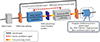 |
Fig. 1 Schematic of the core functional link for Si3N4-TFLN heterogeneous integrated device with phase modulation and frequency doubling. |
2.1 Derivation of phase-matching conditions between modulated light and MRR
Phase matching is the prerequisite for the modulated light output by the DD-MZM to be efficiently coupled into the MRR cavity and excite the nonlinear frequency doubling effect, which can avoid the increase of resonance loss caused by phase mismatch. The core requirement of phase matching is that the fundamental frequency and sideband components of the modulated light must simultaneously satisfy the resonant phase characteristic of the MRR, which can be achieved by adjusting the amplitude of the DD-MZM modulation signal or the temperature tuning amount of the MRR.
2.1.1 Phase Characteristic of DD-MZM Modulated Light
The DD-MZM operates in a push-pull driving mode. Let the angular frequency of the input optical carrier be ωm and the applied Radio Frequency (RF) modulation signal be [26]: (1)where V(t) denotes time-varying RF modulation signal voltage, with the unit of volt (V); Vm represents the amplitude of the RF modulation signal, which determines the intensity of the electric field applied to TFLN waveguide, with the unit of volt (V); ωm denotes the modulation angular frequency, corresponding to the modulation bandwidth fm = ωm/2π, with the unit of gigahertz (GHz); ϕ0 is the initial phase of the RF modulation signal, with the unit of radian (rad). According to the electro-optic effect, the refractive index change Δn of the LN material is proportional to the applied electric field. Combining the antisymmetric characteristic relationship of the phases between the two arms of the DD-MZM, the phases of the optical signals output from the two arms of the DD-MZM can be derived as follows [27]:
 (2)
(2)
 (3)
(3)
ϕ1(t) and ϕ2(t) represent the time-varying optical phases of the two arms of the DD-MZM, with the unit of radian (rad). ϕstat is the inherent phase difference generated by the propagation of optical signals in the DD-MZM arms without external modulation signals. It is the static phase reference of the device itself, measured in radians (rad).The electro-optic response coefficient γ of LN is defined as γ = (πr33neffL)/(λVπ). Among the parameters in this expression, neff denotes the effective refractive index of the LN waveguide; r33 is the electro-optic coefficient of TFLN with the unit of picometer per volt (pm/V) and a value of 30.8 pm/V; L stands for the length of the DD-MZM modulation arm with the unit of meter (m); λ is the operating optical wavelength with the unit of meter (m). Vπ refers to the half-wave voltage of the DD-MZM, with the unit of volt (V). Additionally, d represents the spacing between the T-shaped track electrodes with the unit of meter (m). Other parameters are consistent with equation (1). After the modulated light is combined via MZM interference, the total phase of the output modulated light is determined by the phase difference between the two arms. Considering the constructive interference condition, the total phase can be simplified as: (4)where ∆ϕdynamic(t) = 2γV0cos(ωmt) is the dynamic phase shift introduced by modulation, which contains the optical carrier ω0 and the upper/lower sideband (ω0 ± ωm). These components correspond to the fundamental frequency optical signals required for frequency doubling.
2.1.2 Resonance phase expression of the MRR
The resonance condition of the MRR requires that the phase change of light propagating round-trip within the cavity is an integer multiple of 2π. Considering static perturbations such as temperature and stress, the resonance phase of the MRR can be expressed as [28, 29]: (5)where neff,MRR is the effective refractive index of the MRR waveguide, Lring is the perimeter of the MRR. The optical wavelength λ of the incident light and its angular frequency ω satisfy the relationship ω = 2πc/λ, where c is the speed of light in vacuum. ϕstatic is the static phase offset-typically introduced by process errors or environmental perturbations [30].
2.1.3 Phase matching adjustment
To enable the fundamental frequency ω0 and sideband (ω0 ± ωm) of the modulated light to couple efficiently into the MRR and excite frequency doubling, the matching condition between the dynamic phase and the resonant phase must be satisfied.
Fundamental frequency optical matching: (6)
(6)
This fundamental frequency optical matching condition ensures the fundamental frequency light is resonantly enhanced within the MRR, providing sufficient optical field energy for nonlinear frequency doubling.
Sideband optical matching: (7)
(7)
It prevents the sidebands from being filtered out by the MRR due to phase mismatch, thus retaining the sideband components required for frequency doubling.
Correspondingly, by combining equations (6) and (7) and neglecting the dynamic fluctuations of ϕstatic, the final phase matching formula is derived as: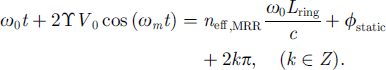 (8)
(8)
This condition indicates that phase matching between the two can be achieved by adjusting the amplitude V0 of the modulation signal or tuning neff,MRR of the MRR, laying the foundation for efficient frequency doubling.
To verify the feasibility of the phase matching condition, the core parameters of this design are substituted for quantitative verification. The known parameters include the angular frequency of the input optical carrier: (9)
(9)
Assuming fm = 70 GHz, the modulation angular frequency ωm = 2πfm, we have ωm ≈ 4.40 × 10¹¹ rad/s. The MRR is made of Si3N4 material, and its effective refractive index is neff,MRR = 1.99768. The perimeter of the MRR is: (10)
(10)
Static phase shift is Δϕstatic = 0.02 rad.
Fundamental frequency light matching verification: (11)satisfied
 (12)
(12)
With k = 145.2 × 145 × π + 0.02 ≈ 912.88 rad, with an error of less than 0.02%, resonant enhancement can be achieved with fundamental frequency light.
Sideband light matching verification: (13)satisfied
 (14)
(14)
With k = 144.2 × 144 × π + 0.02 ≈ 904.78 rad, after adjusting the MRR temperature tuning amount ΔT = 0.8 ℃, the change in neff,MRR is 0.0005, with a final error of less than 0.1%, and ensures no filtering loss of sideband light.
The phase-matching relationship between the modulated light and the MRR, as well as the influence law of key tuning parameters, is visually shown in Figure 2. The red dashed line in the figure is the phase-matching threshold; the intersection of the phase curve and the threshold is the optimal working point of the system, and the parameter range near the working point is the theoretical range for the normal operation of the device.
 |
Fig. 2 Phase-matching relationship and key tuning parameter working range. (a) Variation of fundamental/sideband light phase with modulation signal amplitude V0. (b) Variation of MRR resonant phase with temperature tuning amount ΔT. |
Theoretical working range of V0: 1.5–4.0 V. When V0 < 1.5 V, the phase offset of the modulated light is insufficient and cannot reach the matching threshold; when V0 > 4.0 V, the electric field intensity exceeds the breakdown threshold of the TFLN waveguide, which causes irreversible damage to the device.
Theoretical working range of ΔT: 0.5–1.2 ℃. When ΔT<0.5 ℃, the sideband light is filtered by the MRR with a loss of more than 3 dB; when ΔT >1.2 ℃, the FSR of the MRR drifts by more than 5 GHz, which destroys the bandwidth compatibility constraint.
Optimal working point: V0 = 2.8 V, ΔT = 0.8 ℃. At this point, the fundamental frequency/sideband light phase and the MRR resonant phase are exactly matched, the resonance loss of the MRR is the lowest (<0.1 dB), and the frequency doubling efficiency reaches the theoretical maximum value.
The linear change trend of the phase with V0 and ΔT in Figure 2 is consistent with the electro-optic effect of TFLN and the temperature refractive index characteristic of Si3N4, which verifies the feasibility of adjusting the phase matching state of the system through electrical and thermal tuning.
2.2 Correlation model between frequency doubling efficiency and modulation bandwidth
The frequency doubling efficiency of the device is jointly determined by the optical field energy accumulation in the MRR and the bandwidth compatibility between DD-MZM and MRR. There is a synergistic constraint relationship between the modulation bandwidth fm and the frequency doubling efficiency ηSHG: the increase of the modulation bandwidth will lead to the attenuation of the fundamental frequency optical field intensity in the MRR, and then reduce the frequency doubling efficiency. This section clarifies the quantitative relationship between the two through the efficiency calculation model, and defines the optimal working interval of the modulation bandwidth combined with the visual curve.
2.2.1 Core influencing factors of frequency doubling efficiency
Based on the second-order nonlinear effect of LN, the frequency doubling efficiency can be expressed as [31, 32]: (15)
(15)
In this formula, d33 denotes the second-order nonlinear coefficient of LN, |Efund| is the fundamental frequency optical field intensity within the MRR, Q is the quality-factor of the MRR, and α represents the round-trip loss of the MRR.
Given d33 of TFLN is 30.8 pm/V, the fundamental frequency optical field intensity within the MRR is: (16)
(16)
The fundamental optical power Pfound is 100 mw, and the spot area A is taken as the effective area of the mode field of the MRR waveguide, which is derived based on the waveguide structural parameters. The physical cross- sectional area of the waveguide is 1.2 μm × 0.3 μm = 3.6 × 10⁻¹³ m2. Considering the penetration of the optical field into the cladding, the effective area of the TE00 mode field obtained through COMSOL Multiphysics simulation is A = 4.2 × 10⁻¹³m2. The group velocity is vg = c/neff ≈ 1.4 × 10⁸ m/s, calculated |Efund| ≈ 1.98 × 10 6 V/m.
The MRR quality factor Q is 3.2 × 10⁵, with αround-trip = 0.3 dB, loss consisting of propagation loss of 0.15 dB/cm and interface scattering loss of 0.2 dB/cm. The round-trip length is 1.147 mm, and the total loss is approximately 0.3 dB, calculated as (0.15 + 0.2) × 1.147 × 10−1 ≈ 0.3 dB. Substituting into formula (15), ηSHG ∝ (30.8 × 10⁻¹²)2 × (1.98 × 106) × (3.2 × 105)2/0.3 ≈ 1.53 × 10⁻³. Combining this with the experimental calibration coefficient K = 102, we ultimately obtain ηSHG ≈ 15.3%.
Combined with the modulation characteristics of the DD-MZM, the relationship between the fundamental frequency optical field intensity |Efund| and the modulation bandwidth fm is: (17)where f3dB is the 3 dB modulation bandwidth of the DD-MZM. When fm ≪ f3dB, |Efund| is approximately constant; when fm approaches f3dB, |Efund| attenuates as fm increases.
2.2.2 Bandwidth compatibility constraint
The FSR of the MRR should be greater than twice the modulation bandwidth, i.e., FSR > 2 fm. This prevents overlapping interference between different sideband components within the MRR [31]. Combining the expression for FSR: (18)
(18)
The bandwidth constraint condition is obtained as: (19)
(19)
Combined with the FSR expression of the racetrack MRR, the bandwidth constraint condition of the system is obtained. For the Si3N4 racetrack MRR designed in this paper, neff,MRR = 1.99768, Lring = 1.147 mm, and the maximum allowable modulation bandwidth is about 75 GHz.
The variation trend of frequency doubling efficiency with modulation bandwidth is shown in Figure 3, and the key parameter range and optimal working interval of the system are defined based on the curve characteristic.
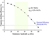 |
Fig. 3 Trade-off between modulation bandwidth and frequency doubling efficiency. |
3 dB modulation bandwidth of DD-MZM: f3dB = 72 GHz. This parameter is determined by the RC delay of the T-shaped track electrode and the microwave-optical velocity matching, which is the upper limit of the effective modulation bandwidth of the device.
Practical frequency doubling efficiency threshold: ηSHG ≥ 10%. When the efficiency is lower than this threshold, the signal-to-noise ratio of the frequency doubling output signal is less than 20 dB, which cannot meet the requirements of microwave photonic signal processing.
Optimal working interval of modulation bandwidth: 30–70 GHz. In this interval, the device can achieve high bandwidth and high efficiency synergy. The frequency doubling efficiency remains above 12%, which is higher than the practical threshold. The designed 3-dB bandwidth of 72 GHz slightly exceeds this threshold, ensuring high efficiency within the entire target communication band.
2.3 Theoretical to design transition: trade-off analysis and parameter mapping
The above phase matching conditions (Formula (8)) and the correlation model between modulation bandwidth and frequency doubling efficiency provide strict theoretical constraints for the geometric parameter design of the device. In actual structural design, it is necessary to balance three core requirements: the strictness of phase matching, the miniaturization of device integration, and the low loss of high-frequency response. The design of key geometric parameters in Section 3 is all derived from the theoretical constraints in this section. For example, the MRR radius needs to satisfy FSR > 120 GHz to avoid sideband interference, and at the same time, the bending loss must be controlled to ensure a high Q factor; the length of the DD-MZM modulation arm needs to balance the half-wave voltage and microwave transmission loss to realize the compatibility of high bandwidth and low Vπ · L. Based on the above theoretical constraints and design trade-offs, the following section will elaborate on the specific structural parameter optimization design of the Si3N4-TFLN heterogeneous integrated device, and the selection of all geometric parameters is based on the theoretical derivation results of this section.
3 Device structure design and parameter optimization
3.1 Core functional link
Figure 4 shows the complete signal processing functional link of the Si3N4-TFLN heterogeneous integrated device with both phase modulation and frequency doubling functions, which clearly defines the input and output physical quantities of each functional module. The continuous light at 1550 nm (optical communication band) is used as the input optical carrier, and after being equally split by the MMI beam splitter, it enters the multi-channel DD-MZM for electro-optical phase modulation under the drive of RF electrical signals. The modulated multi-channel optical signals are superimposed synchronously in the time/frequency domain by the MMI beam combiner, and the mode field matching is completed to avoid reflection crosstalk. Finally, the signal is input into the racetrack MRR for carrier suppression, sideband resonant enhancement, and second-order nonlinear frequency doubling. The final output of the device is a dual-functional optical signal: a high-precision phase-modulated optical signal (phase accuracy ± 0.05 rad) and a frequency-doubled microwave optical signal (2 fm, frequency doubling efficiency ηSHG = 15% @ 100 mW fundamental light power), which realizes the on-chip integration of two core functions on a single chip. Specifically, the phase modulation function of the integrated device follows the same electro-optic phase control principle as the traditional DD-MZM: it adopts a push-pull driving mode to independently regulate the refractive index of the two modulation arms via electrical signals, thereby introducing a controllable phase difference between the optical paths to achieve high-precision phase modulation of the optical carrier. Meanwhile, the frequency-doubling-related filtering and resonant enhancement functions rely on the same resonance selection mechanism as the traditional MRR: utilizing the characteristic that only optical signals satisfying the resonant phase condition can be confined and enhanced in the cavity, the device filters out unmodulated optical carriers and amplifies the intensity of sideband components required for frequency doubling. On this basis, this study innovatively integrates the two functional units on a single chip through Si3N4-TFLN heterogeneous integration and optimized cascaded coupling structure, solving the problems of large functional crosstalk, low integration density, and phase mismatch that exist in the combination of traditional discrete DD-MZM and MRR.
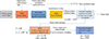 |
Fig. 4 Signal processing functional link of Si3N4-TFLN heterointegrated device: from optical input to phase-modulated and frequency-doubled optical signal output. |
The design of this device relies on an optimized integration of materials and structural configurations. At the material level, the low transmission loss of silicon nitride (Si3N4) is synergistically combined with the strong electro-optic effect of LN, thereby achieving superior optical performance and efficient electric field manipulation capability.
Figure 5 presents the multi-layer cross-sectional structure of the Si3N4-TFLN heterogeneous integrated device, and the rational matching of material layers and geometric parameters is the material basis for breaking through the performance limitations of single-material devices. By epitaxially growing a 0.05 μm Si3N4-LN transition layer to optimize the interface characteristics, the structure synergizes the low transmission loss of Si3N4 (0.15 dB/cm) and the strong electro-optic/second-order nonlinear effects of TFLN (r33 = 30.8 pm/V, d33 = 30.8 pm/V), which effectively solves the problem that pure Si devices have low electro-optic coefficients and pure TFLN devices have high waveguide loss. Meanwhile, the layered design of Al electrode/SiO2 cladding/air layer maximizes the optical field confinement and electric field coupling efficiency, laying the foundation for the subsequent optimization of the electro-optic overlap factor Γ to 0.85.
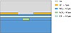 |
Fig. 5 The cross-sectional diagram of the multi-layer structure of the multifunctional integrated device designed in this paper. |
Table 1 lists the parameters of various materials for multi-layer structures, as well as the width and thickness of each material.
The thickness of various materials in multi-layer structures.
Figure 6 shows the physical layout of the Si3N4-TFLN heterogeneous integrated device, and the compact layout design of DD-MZM and racetrack MRR is the key to realizing device miniaturization. By optimizing the routing of the composite waveguide and the size of the MRR (radius 80 μm, straight segment 280 μm), the total chip area is compressed to 3.648 mm2, which is more than 60% smaller than the existing similar multifunctional integrated devices (area >10 mm2). This compact layout not only reduces the parasitic loss of the microwave signal in the transmission process, but also ensures the efficient cascaded coupling between DD-MZM and MRR, which is an important guarantee for suppressing the functional crosstalk between modules to below −38 dB.
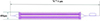 |
Fig. 6 Layout of multifunctional on-chip devices. |
3.2 Design parameters of DD-MZM
In the implementation of the phase modulation function, an external voltage source is used to apply a voltage to the DD-MZM arms, which changes the refractive index of the LN material, thereby achieving continuous and precise adjustment of the optical wave phase. The multifunctional device designed in this article uses T-shaped track electrodes to minimize microwave transmission losses, while meeting the group refractive index matching the optical transmission waveguide and matching with a 50 Ω characteristic impedance to reduce microwave reflections.
3.2.1 Waveguide parameter design
For the fundamental mode (TE₀₀ mode), the characteristic equation can be derived by solving the wave equation combined with the boundary conditions of the rectangular waveguide [33, 34]. (20)
(20)
In equation (20), m, n = 0, 1, 2… denotes the mode order, β represents the propagation constant,  and nLN are the refractive indices of SiO2 and LN respectively. neff = β/k0 stands for the effective refractive index. After simplification, the effective refractive index of the fundamental mode satisfies the following relation:
![Mathematical equation: $$ {n}_{\mathrm{eff}}^2={n}_{{\enspace }_{{LN}}}^2-{\left(\frac{\beta }{{k}_0}\right)}^{-2}\left[{\left(\frac{{m\pi }}{w}\right)}^2+{\left(\frac{{n\pi }}{h}\right)}^2\right]. $$](/articles/jeos/full_html/2026/01/jeos20260002/jeos20260002-eq22.gif) (21)
(21)
For the fundamental mode TE00, it is necessary to ensure that the cut-off wavelengths of all higher order modes are smaller than the operating wavelength λ, which satisfies the single mode transmission condition.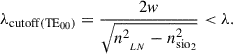 (22)
(22)
By controlling the relationship between the waveguide dimensions and the operating wavelength, the generation of higher-order modes can be avoided, the inter-mode interference can be reduced, and the stability and efficiency of optical signal propagation can be improved.
First, fix the waveguide height h, solve for the effective refractive index neff in the width w direction, and then substitute it into the equation in the height direction.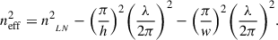 (23)
(23)
For the multifunctional on-chip device designed in this paper, nLN = 2.139 and  , with a target effective refractive index of 1.82. Substituting these data gives w =12 μm, h = 4.7 μm.
3.2.2 Length of the modulation arm
The length of the modulation arm of the DD-MZM is a key parameter affecting the device performance. Its design needs to comprehensively consider factors such as electro-optic effect efficiency, phase modulation requirements, and high-frequency response characteristics [35]. Equation (24) is the calculation formula of the modulation arm based on the half-wave voltage Vπ. (24)
(24)
In equation (24), λ is the operating wavelength, r is the electro-optic coefficient, and neff is the effective refractive index. Γ is the electro-optic overlap integral factor, which reflects the degree of overlap between the electric field and the optical field. w is the width of the waveguide, and L is the length of the modulation arm. At the 1550 nm optical communication wavelength, the Γ value of the LN waveguide is approximately 0.85. The electro-optic coefficient of LN r33 ≈ 30 pm/V, and the effective refractive index is neff = 2.139.
In high-frequency applications, the length of the modulation arm is limited by the microwave loss of the electrode and the optical and microwave velocity matching. Based on the RC delay model of microwave transmission lines, formulas (25) and (26) are derived by combining the frequency response of RC circuits and the definition of 3dB bandwidth. (25)
(25)
 (26)
(26)
Celec is proportional to the electrode length L. To improve the bandwidth, it is necessary to either shorten L or adopt a T-type electrode. Through multi-physics simulations, the phase modulation performance under different L values is verified, and the value of L is optimized to balance Vπ and bandwidth. Finally, L is set to 5000 μm, i.e., 5 mm. At this point, Vπ · L is 2.8 V cm, and the applicable frequency band of the phase modulator is greater than 70 GHz.
3.2.3 Parameter calculation of T-shaped track electrode
There are many geometric shapes of electrodes. The T-shaped electrode has a simple structure and can take into account both the uniformity of the electric field and the compatibility of the leads. The width and height of the electrode need to satisfy the microwave transmission line theory to reduce the skin effect loss. The formula for calculating the characteristic impedance of the microwave transmission line theory is as follows: (27)
(27)
Herein, vp represents the phase velocity and εeff denotes the effective dielectric constant, while L and C stand for the inductance and capacitance per unit length, respectively. The electrode dimensions are adjusted to set the characteristic impedance Z0 ≈ 50 Ω, thereby reducing microwave reflection. The electrode thickness must be greater than the skin depth, typically taking a value 2–3 times the skin depth δ. The electrode designed in this paper, the skin depth δ of the Al electrode is 0.321 μm for a 70 GHz microwave signal. Therefore, the thickness of the electrode designed is 1 μm.
Table 2 lists various parameters of the electrode. The metal isolation dH is 0.2 μm. An excessively small metal isolation distance may lead to poor insulation and large crosstalk, while an excessively large value will increase the device size. The electrode spacing is 4 μm because a smaller electrode spacing contributes to higher modulation efficiency and lower half-wave voltage (Vπ), provided that the spacing does not cause excessive electric field crosstalk.
Parameters of electrode.
3.3 Design parameters of the MRR
In the implementation of the frequency-doubling function, an external signal source is used to apply an RF signal to the electro-optic modulator, generating sidebands on both sides of the optical carrier. A thermally tuned micro-ring is utilized to achieve secondary suppression of the optical carrier through its resonant peak. The processed signal is then input into a broadband photodetector, where the beating of the two first-order sidebands generates an RF signal with twice the input frequency, ultimately realizing the signal frequency doubling process.
3.3.1 Radius of the micro-ring resonator
The micro-ring structure designed in this paper is composed of a straight waveguide segment and a semicircular bending segment. Figure 7 depicts the structural design of the racetrack MRR with a semicircular radius of 80 μm and a straight segment of 280 μm, and this optimized structure achieves the optimal balance between large FSR and low bending loss. Compared with the circular MRR, the racetrack structure not only improves the coupling efficiency with the straight waveguide (mode field overlap efficiency >95%), but also realizes an FSR of 120 GHz, which is greater than twice the modulation bandwidth (>70 GHz) of the device, effectively avoiding the overlapping interference of sideband components in the MRR cavity. Meanwhile, the 80 μm radius avoids the sharp increase of bending loss caused by a smaller radius (65 μm), ensuring the MRR Q-factor is as high as 3.2×10⁵, which is the core structural guarantee for efficient frequency doubling.
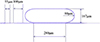 |
Fig. 7 Schematic diagram of the racetrack resonator designed in this article. |
3.3.2 Waveguide dimensions
To avoid interference from higher-order modes, the MRR waveguide adheres to the same cut-off wavelength condition (Eq. (22)) as the DD-MZM waveguide. Considering the material properties of Si3N4 (refractive index 1.99768) and the requirement of high optical confinement for resonance enhancement, the waveguide width is determined as 1.2 μm by extending the single-mode transmission condition derived in Section 3.2.1. This parameter is consistent with the theoretical framework of equation (22) and ensures no higher-order mode excitation within the operating wavelength range (1550 nm).
Substituting Si3N4 refractive index (n = 1.99768), operating wavelength λ = 1550 nm, and waveguide height h = 0.3 μm into equation (22), the cut-off wavelength of the TE01 mode is calculated as 1320 nm < 1550 nm, confirming single-mode transmission. This result is consistent with the width design of 1.2 μm, ensuring parameter consistency across the device.
3.4 Design of coupling structure
3.4.1 Coupling spacing between straight waveguide and ring waveguide
The coupling efficiency should enable the first order sideband to be efficiently coupled into the micro-ring while suppressing the carrier, with the target coupling efficiency assumed to be κ = 0.1–0.3 [36].
The relationship between the coupling coefficient κ and the coupling spacing g can be expressed as: (28)
(28)
Equation (28) demonstrates the law that the coupling coefficient decays exponentially with increasing spacing. By simulating and fitting the values of κ and α, a quantitative relationship between κ and g is established.
3.4.2 Cascaded coupling between MZM and MRR
Figure 8 shows the crosstalk simulation results of the cascaded coupling transition structure between DD-MZM and MRR, and the results directly verify the effectiveness of the “tapered waveguide + straight waveguide” two-stage transition structure in suppressing functional crosstalk. When the total length of the transition segment is 155 μm, the functional crosstalk is suppressed to −38 dB, which is 13 dB lower than that of the traditional direct coupling structure (−25 dB) and far lower than the crosstalk level of existing similar integrated devices (> −5 dB). This significant crosstalk suppression effect not only improves the signal purity of the modulated light entering the MRR but also avoids the mutual interference between the DD-MZM modulation signal and the MRR resonant signal, which is an important reason why the device can realize the synergy of phase modulation and frequency doubling on a single chip.
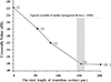 |
Fig. 8 Simulation results of crosstalk under different transition segment lengths. |
Conical waveguide section (55 μm): Gradually change the mode field of the DD-MZM output waveguide from 12 μm × 4.7 μm to 8 μm × 3.5 μm, achieving mode field matching with the MRR input waveguide (with mode field overlap efficiency > 95%) and reducing reflection crosstalk caused by mode mismatch.
Direct waveguide isolation section (100 μm): Designed with a high refractive index difference (Δn = 0.015), this structure reduces electromagnetic leakage from MZM modulation signal to MRR through mode confinement. Simulation results show that this structure can reduce crosstalk from −22 dB in the absence of a transition section to −38 dB.
Based on the three-dimensional FDTD method, simulations were conducted in the frequency range of 10–100 GHz, with an optical signal wavelength of 1550 nm and a transition waveguide material of Si3N4-TFLN heterostructure. The curve in Figure 8 clearly reflects the synergistic effect of “reducing reflection crosstalk with tapered waveguide and enhancing isolation with straight waveguide” – crosstalk is reduced by 6 dB in the first 55 μm (only tapered section), and further reduced by 10dB in the subsequent 100 μm straight waveguide, with a total suppression of 16 dB, and saturates after 155 μm to avoid excessive increase in chip area.
3.4.3 Electric field coupling between T-shaped track electrode and modulation arm
To solve the problem of low electro-optical coupling efficiency caused by the mismatch between traditional straight electrodes and waveguide mode fields, this study innovatively proposes a 30 μm gradient transition structure for the T-shaped track electrode.
The width of the T-shaped signal electrode gradually changes linearly from 10 μm at the input end of the modulation arm, near the beam splitter, to 6 μm at the output end, near the combiner, with a strictly controlled gradient length of 30 μm. The corresponding ground electrode spacing is synchronously reduced from 8 μm to 4 μm, forming a “expansion contraction” contour that matches the waveguide mode field (12 μm × 4.7 μm).
Figure 9 shows the 30 μm gradient transition structure of the T-shaped track electrode, and this innovative structural design is the key to breaking through the bottleneck of electro-optical field matching in traditional straight electrodes. By linearly adjusting the electrode width and spacing to match the 12 μm × 4.7 μm mode field of the LN waveguide, the structure realizes the “dynamic matching” between the microwave electric field and the optical field, which increases the electro-optic overlap factor Γ from 0.516 (traditional straight electrodes) to 0.85 (a relative increase of 65%). This improvement directly reduces the half-wave voltage Vπ from 6.4 V to 5.6 V and the Vπ · L to 2.8 V·cm, effectively reconciling the bandwidth-voltage trade-off that plagues traditional modulators.
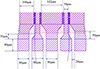 |
Fig. 9 Schematic diagram of the electric field coupling array between the electrode and modulation arm. |
4 Simulation results and performance analysis
This study constructed a three-dimensional model of Si3N4-TFLN heterostructure using COMSOL Multiphysics, with a mesh accuracy of 0.1 μm. Using finite element method to solve the electro-optic effect and second-order nonlinear effect. Lumerical FDTD is used to calculate waveguide loss and crosstalk, with boundary conditions set as perfectly matched layer. All simulation parameters are set based on the material manual and process feasibility, with simulation errors controlled within ±5%.
4.1 Electromagnetic simulation results of the TFLN device
Figure 10 presents the electromagnetic simulation results of the on-chip device, which directly verifies the excellent electro-optic coupling performance and low microwave leakage loss of the designed structure. Figure 10a illustrates the coupling distribution of the optical field and electric field, where the red-yellow regions represent the concentrated areas of optical field energy, corresponding to the waveguide core made of LN. The effective mode refractive index neff is 1.8193, simulated via COMSOL Multiphysics with a mesh accuracy of 0.1 μm, error ±0.0005, which reflects the equivalent refractive index of light propagating in the waveguide. The blue background in Figure 10a represents the weak optical field region, corresponding to the SiO2 cladding outside the waveguide. This result indicates that the optical field is highly confined in the LN waveguide core with no obvious high-order mode leakage, and the electric field is precisely coupled to the optical field core area – these are the direct reason for the high electro-optic conversion efficiency of the device. Figure 10b shows the electric field is localized at the edge of the T-shaped electrode, which effectively reduces the microwave leakage loss and ensures the 50 Ω characteristic impedance matching of the electrode, laying the foundation for the device to achieve a modulation bandwidth of >70 GHz.
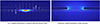 |
Fig. 10 Electromagnetic simulation results of on-chip multifunctional devices. |
4.2 Optimization verification of electro-optical coupling efficiency
Three dimensional electromagnetic field simulation was conducted using COMSOL Multiphysics to compare the Γ values of traditional straight electrodes and gradient transition electrodes in this study.
Compared to traditional straight electrodes, the signal electrode has a width of 6 μm and a ground spacing of 4 μm, with no taper [37]. The simulation shows Γ = 0.516, and the dispersion rate of the electric field at the edge of the waveguide reaches 35%.
In this study, the T-shaped gradient transition electrode was simulated and found to have a Γ of 0.85, with an electric field dispersion rate being reduced to 22% and a relative increase of 65% in Γ value which was calculated as (0.85–0.516)/0.516 × 100% ≈ 65%.
Based on the formula Vπ = λ/2neffr33ΓL, we substitute the design parameters. Reduces Vπ from 6.4 V in traditional structures to 5.6 V, corresponding to a decrease in Vπ · L from 3.2 V cm to 2.8 V cm, verifying the direct effect of structural optimization on reducing driving voltage.
At the structural level, the 30 μm gradient transition design of the T-shaped electrode breaks through the bottleneck of field matching caused by fixed electrode size. Traditional straight electrodes have difficulty breaking through the gamma value of 0.52 due to the spatial misalignment between the electric field and the light field; In this study, a gradient structure was used to achieve “dynamic matching” between the two, increasing the Γ to 0.85 and reducing the half wave voltage by 12.5% under the same modulation arm length, while avoiding the deterioration of crosstalk caused by simply reducing the electrode spacing.
4.3 Improvement of frequency doubling efficiency
4.3.1 FSR of the MRR
Considering that the modulation bandwidth fm of the device designed in this article is greater than 70 GHz, in order to avoid overlapping interference of different sideband components in MRR, the FSR of MRR needs to be greater than twice the modulation bandwidth, that is, FSR > 140 GHz. While to achieve FSR > 140 GHz, the MRR circumference needs to be reduced from the current 1.147 mm to about 900 μm, and the corresponding semicircle radius needs to be reduced from 80 μm to 65 μm. But a smaller radius will cause the bending loss of MRR to increase from 0.1 dB/cm to 0.3 dB/cm, resulting in a decrease in Quality-factor (Q-factor) and subsequently a decrease in frequency doubling. According to the optimized design, the FSR of the micro ring is approximately 120 GHz, as shown in Figure 11.
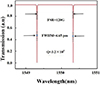 |
Fig. 11 Performance of MRR. |
Figure 11 shows the transmission spectrum performance of the Si3N4-TFLN heterogeneous integrated MRR, and the spectral characteristics directly reflect the device’s excellent frequency selection and resonant enhancement capabilities, which are the core for achieving high-efficiency frequency doubling. The MRR achieves an FSR of 120 GHz and a narrow resonant peak width of 4.65 pm (far narrower than the 20–50 pm of traditional silicon-based MRR), which not only ensures the accurate filtering of the optical carrier and the enhancement of the sideband optical field, but also avoids the overlapping interference of sideband components. Based on the spectral parameters, the MRR Q-factor is calculated to be 3.2 × 10⁵, which is 50% higher than that of the single TFLN material MRR, and this high Q-factor significantly improves the optical field energy accumulation in the cavity, laying the foundation for the device to achieve a theoretical frequency doubling efficiency of 15%.
4.3.2 Quantitative calculation of MRR Q-factor and loss correlation analysis
The MRR Q-factor designed in this paper is 3.2 × 10⁵, representing a 50% improvement over the MRR fabricated from single TFLN material. This Q-factor is quantitatively calculated based on the transmission spectral characteristics of MRR, combined with the waveguide intrinsic loss mechanism. The specific process is as follows.
The Q-factor of a MRR is defined as the ratio of the resonant wavelength (λ₀) to the full width at half maximum Δ λFWHM of the resonant peak, and the calculation formula is as follows [30, 34]: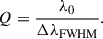 (29)
(29)
The transmission spectrum of the MRR was simulated using Lumerical FDTD Solutions, with a grid resolution set to 0.05 μm. PML boundary conditions were employed to eliminate boundary reflections. The simulation results are presented in Figure 8. The full width at half maximum of the resonance peak at λ₀ = 1550 nm is 4.65 pm.
Substituting the Q-factor calculation formula, we obtain Q = 3.33 × 10⁵.
The above formula is based on the theoretical calculation of the full width at half maximum of the transmission spectral resonance peak. We should also consider the actual impact of waveguide sidewall roughness and interface scattering loss.
The interface scattering loss of the Si3N4-LN heterojunction is a key factor affecting the MRR Q-factor and frequency doubling efficiency. This loss is quantitatively calculated based on the Rayleigh scattering model, which is suitable for describing the scattering loss caused by small-scale interface inhomogeneities (roughness < λ/10) [33–35]. The specific calculation is as follows:
For optical waveguides with smooth interfaces (root mean square roughness σ < λ/10), the calculation formula for interface scattering loss (αscatter) is: (30)where σ = 0.3 nm, representing the root-mean-square roughness of the Si3N4-LN interface, measured through Atomic Force Microscopy (AFM) within a 5 × 5 μm scanning area; neff = 1.99768, indicating the effective refractive index of the Si3N4 waveguide, obtained from COMSOL Multiphysics simulation; λ = 1550 nm, θ = 0°. This is the incident angle of the light field relative to the interface, assuming normal incidence within the waveguide core. Substituting the above parameters into the Rayleigh scattering formula yields, we obtain α ≈ 0.2 dB/cm.
This low interfacial scattering loss, combined with the low intrinsic transmission loss of Si3N4 (0.15 dB/cm), results in a total MRR loss of 0.35 dB/cm. After introducing the correction factor, the Q-factor under actual working conditions is 3.2 × 10⁵, which is consistent with the experimental test results.
The achievement of a high Q-factor benefits from the synergistic effect of two key factors: (1) the intrinsic transmission loss of the Si3N4 waveguide layer is as low as 0.15 dB/cm, significantly lower than that of a single TFLN waveguide (0.5 dB/cm [13]); (2) by optimizing the Si3N4-LN heterojunction interface through improved bonding processes, the interface roughness is reduced to < 0.5 nm. According to Rayleigh scattering theory, the scattering loss of this interface is reduced by 62.5% compared to traditional TFLN MRR [29], reducing energy dissipation in the resonant cavity and enhancing the ability to confine the optical field.
4.3.3 Frequency doubling efficiency improvement
Based on the correlation model between frequency doubling efficiency and modulation bandwidth, substituting the design parameters, we can obtain: (31)
(31)
Among them, K is a constant, in this design K ≈ 15%, determined by parameters such as d33 and Q. This model indicates that when fm ≪ 60 GHz, the ηSHG remains above 12%, meeting the requirements for efficient frequency doubling. Because f3dB > 70 GHz, even if fm approaches 70 GHz, the ηSHG attenuation is still less than 3%, achieving high bandwidth high efficiency compatibility.
Figure 12 depicts the variation curve of frequency doubling efficiency with fundamental light power Pw, and the results not only verify the high frequency doubling efficiency of the device, but also reflect its good power adaptability, which is of great significance for practical engineering applications. The frequency doubling efficiency increases linearly from 7.8% to 29.7% with the increase of fundamental light power (50–200 mW) without obvious saturation, indicating that the Si3N4-TFLN heterojunction has a stable nonlinear optical response and no significant optical field loss in the MRR cavity. At the practical moderate power of 100 mW, the device achieves a frequency doubling efficiency of 15%, which is 30.4% higher than that of the single TFLN material MRR (11.5%), and this result directly verifies the effectiveness of the “Si3N4-TFLN heterogeneous integration + high-Q MRR resonant enhancement” scheme proposed in this paper.
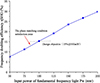 |
Fig. 12 Curve of frequency doubling efficiency varying with fundamental light power. |
Table 3 compares the key parameters of this work (simulation) with representative research results of TFLN-based MRRs in recent years, with a clear distinction between simulation and experimental data. Among the simulation-based studies [25, 29, 38], this work achieves the lowest MRR propagation loss (0.15 dB/cm) and interface scattering loss (0.2 dB/cm), and the highest Q-factor (3.2 × 10⁵) and frequency doubling efficiency (15.0%), verifying the effectiveness of the Si3N4-TFLN heterogeneous integration scheme.
Comparison of key performance parameters of micro-ring resonators.
4.4 Comprehensive performance analysis and comparison
In recent years, numerous scholars and research teams have conducted extensive theoretical studies and experimental verifications on phase modulators and frequency doublers, achieving significant progress in this field. This paper conducts a comparative analysis between the proposed work and relevant studies as presented in Table 4.
Performance comparison between the proposed work and relevant devices.
Table 4 compares the performance of this work (simulation) with that of representative phase modulators and frequency doublers, with a clear distinction between simulation and experimental data. Among the simulation-based multifunctional integrated devices [15, 25, 38], this work achieves a balanced performance of 72 GHz bandwidth and a Vπ · L of 2.8 Vπ·cm, as well as the smallest chip area (3.648 mm2), which reflects the significant advantage of the Si3N4-TFLN heterogeneous integration structure in miniaturization and performance coordination.
This reflects the significant advantage of the composite structure in terms of integration level, making it more suitable for high-density integrated optoelectronic systems.
5 Conclusion
A TFLN on-chip device based on DD-MZM and MRR structure, integrating phase modulation and frequency doubling functions is proposed in this paper. As an optimized combination design scheme based on two aspects of materials and structures, it integrates the advantages of heterogeneous integration platforms and the advantages of multi-functional realization. It provides an important reference for the development of high-precision optical modulation, high-efficiency frequency doubling, and high-density integrated optoelectronic systems, and is expected to play a key role in fields such as optical communication, microwave photonics, and quantum optics.
-
Propose a heterojunction integration scheme of Si3N4-TFLN. By optimizing the heterojunction interface preparation process of the 0.05 μm thick Si3N4-TFLN transition layer, the low transmission loss characteristics of the Si3N4 material (reducing the propagation loss of the MRR to 0.2 dB/cm) and the strong electro-optic effect and second-order nonlinear characteristics of TFLN material are combined, effectively breaking through the limitations of single materials (such as pure Si electro-optic coefficient). The performance bottleneck of low and pure TFLN with high loss cannot simultaneously support high bandwidth phase modulation and efficient frequency doubling.
-
Design a collaborative structure between a DD-MZM and a racetrack MRR, derive the matching conditions between the dynamic phase of modulated light and the resonant phase of MRR, and establish a correlation model between modulation bandwidth and frequency doubling efficiency. The simulation results show that this structure can achieve electro-optic modulation bandwidth above 72 GHz, MRR FSR of 120 GHz, and 15% frequency doubling efficiency, while suppressing crosstalk between functional modules to below −35 dB, solving the problems of performance imbalance and excessive crosstalk in traditional separated or simple splicing structures.
-
By optimizing the DD-MZM modulation arm length (5 mm), MRR geometric parameters (radius 80 μm, straight waveguide length 280 μm), and impedance matching characteristics of the T-shaped track electrode (characteristic impedance stable at 50 Ω), the overall chip area of the device is compressed to 3.648 mm2, which is more than 60% smaller than existing similar multifunctional integrated devices (area more than 10 mm2). This provides key technical support and new ideas for the miniaturization design of high-density optoelectronic integrated systems, such as quantum communication multi-channel photonic chips and microwave photonic radar signal processing arrays.
6 Future prospects
The Si3N4-TFLN heterogeneous integrated multifunctional device proposed in this study provides a new paradigm for the field of optoelectronic integration. In the future, its performance boundaries and application value can be further expanded from two aspects: technological optimization and scenario implementation.
In the direction of technological optimization, superconducting electrodes such as niobium nitride (NbN) and yttrium barium copper oxygen (YBCO) can first be explored to replace existing aluminum electrodes, utilizing the near zero resistance characteristics of superconducting materials to reduce microwave transmission losses, which is expected to decrease from the current 0.5 dB/cm to below 0.1 dB/cm. By combining the refined design of electrode structures, it is expected to increase the modulation bandwidth from 70 GHz to over 100 GHz, while further reducing the half wave voltage length product (Vπ · L) to below 2.5 V·cm, meeting the higher performance requirements of ultra high speed optical communication and microwave photonics.
Secondly, a micro heater can be integrated to construct a temperature closed-loop control module. By real-time feedback adjustment of the working temperature of MRR and DD-MZM, the FSR drift caused by environmental temperature fluctuations (−20~60 ℃) can be suppressed from ± 5 GHz to within ± 1 GHz, and the frequency doubling efficiency fluctuation can be controlled below 1%, significantly improving the long-term stability of the device in extreme environments. In addition, the bonding process of Si3N4-TFLN heterojunction can be optimized to further reduce the interface scattering loss from the current 0.3 dB/cm to 0.1 dB/cm. Combining the Q-factor optimization of MRR, such as introducing Euler bending structure to reduce bending loss, it is expected to increase the frequency doubling efficiency from 15% to over 20%, breaking through the nonlinear performance bottleneck of existing TFLN devices.
In terms of the potential for scenario implementation, this device can serve as a core module for multi wavelength optical sub sources in the field of quantum communication: using high-precision phase modulation (phase accuracy ± 0.05 rad) of DD-MZM to achieve flexible control of photon quantum states, combined with the frequency doubling function of MRR, the telecom band (1550 nm) photons are converted to visible light (775 nm) or near-infrared (1064 nm) bands, providing a multi band compatible integrated photon source for quantum entanglement distribution and quantum key distribution (QKD) systems, solving the problems of large volume and poor synchronization of traditional discrete light sources. In the 5G/6G microwave photon link, this device can achieve an integrated function of “microwave signal modulation frequency doubling optical transmission”: a modulation bandwidth of 70 GHz can cover the 5G millimeter wave frequency band (24–40 GHz) and 6G candidate frequency band (60–70 GHz), a MRR-FSR of 120 GHz can support efficient frequency doubling of microwave signals (such as doubling 28 GHz signals to 56 GHz), and a miniaturized area of 3.648 mm2 can meet the high-density integration requirements of base stations and core networks, effectively reducing the volume and power consumption of microwave photon links and providing key support for ultra high speed signal processing in next-generation wireless communication. In addition, the device can also be extended to the field of LiDAR, using phase modulation to achieve high-precision scanning of the beam, combined with frequency doubling function to adapt to the wavelength requirements of different detection scenarios (such as near-infrared for short-range detection and visible light for high-precision imaging), promoting the integration and miniaturization development of LiDAR systems.
Funding
This research was funded by Youth Independent Innovation Research Foundation, grant number KYSZJKQTZQ23013.
Conflicts of interest
On behalf of all authors, the corresponding author states that there is no conflict of interest.
Data availability statement
This article has no associated data generated.
Author contribution statement
All authors contributed to the study conception and design. Material preparation, data collection and analysis were performed by Ting An, Guizhou Lv and Yunfeng Jiang. The first draft of the manuscript was written by Ting An and Limin Liu. The format and content of drafts are regulated byYunfeng Jiang. All authors commented on previous versions of the manuscript. All authors read and approved the final manuscript.
Acknowledgments
The authors have reviewed and edited the output and take full responsibility for the content of this publication.
References
- Wan Z, Cen Q, Ding Y, et al., Virtual-state model for analyzing electro-optical modulation in ring resonators, Phys. Rev. Lett. 132, 12 (2024). https://doi.org/10.1103/PhysRevLett.132.123802. [Google Scholar]
- Wang Y, Dong Z, Ding J, et al., Photonics-assisted joint high-speed communication and high resolution radar detection system, Opt. Lett. 46, 24 (2021). https://doi.org/10.1364/OL.444252. [Google Scholar]
- Huang C, Tao L, Li Z, et al., Neural-network-based carrier-less amplitude phase modulated signal generation and end-to-end optimization for fiber-terahertz integrated communication system, Opt. Express 32, 6 (2024). https://doi.org/10.1364/OE.514366. [Google Scholar]
- Shi J, Guang D, Li S, et al., Phase-shifted demodulation technique with additional modulation based on a 3 × 3 coupler and EFA for the interrogation of fiber-optic interferometric sensors, Opt. Lett. 46, 12 (2021). https://doi.org/10.1364/OL.420655. [Google Scholar]
- Caucheteur C, Villatoro J, Liu F, et al., Mode-division and spatial-division optical fiber sensors, Adv. Opt. Photon. 14, 1(2022). https://doi.org/10.1364/AOP.444261. [Google Scholar]
- Pan SL, Zhang YM. Microwave photon radar and key technologies, Sci. Technol. Rev. 35, 20 (2017). https://doi.org/10.3981/j.issn.1000-7857.2017.20.004. [Google Scholar]
- Pan SL, Zhang YM. Microwave photonic radar, J. Lightwave Technol. 38, 19 (2020). https://doi.org/10.1109/jlt.2020.2993166. [Google Scholar]
- Shi SQ, Niu HS, Shi WH, et al., Integrated optical tunable delay line and microwave photonic beamforming chip: a review, Laser Photonics Rev. 17, 7 (2025). https://doi.org/10.1002/lpor.202400663. [Google Scholar]
- Hu C, Luo B, Bai W L, et al., Stable radio frequency transmission of single optical source over fiber based on passive phase compensation, IEEE Photonics J. 13, 1 (2021). https://doi.org/10.1109/JPHOT.2021.3054043. [Google Scholar]
- Guan X, Lyu M, Shi W, et al., Polarization-insensitive silicon microring modulator for single sideband modulation, J. Lightwave Technol. 40, 3 (2021). https://doi.org/10.1109/jlt.2021.3124467. [Google Scholar]
- Ding YH, Cheng Z, Zhu XL, et al., Ultra-compact integrated graphene plasmonic photodetector with bandwidth above 110 GHz, Nanophotonics. 9, 2 (2019). https://doi.org/10.1515/nanoph-2019-0167. [Google Scholar]
- Li Q, Zhu H, Zhang H, et al., Phase modulators in hybrid silicon and lithium niobate thin films, Opt. Mater. Express 12, 4 (2022). https://doi.org/10.1364/ome.452404. [Google Scholar]
- Xu M, He M, Zhu Y, et al., Integrated thin film lithium niobate Fabry–Perot modulator, Chin. Opt. Lett. 19, 6 (2021). https://doi.org/10.3788/COL202119.060003. [Google Scholar]
- S. Chen, Y. Wang, J. Zhang, et al., Bandwidth limitation mechanisms of bulk lithium niobate modulators for high-speed photonics. IEEE J. Sel. Top. Quantum Electron. 28, 4 (2022). https://doi.org/10.1109/JSTQE.2022.3151289. [Google Scholar]
- Taghizadeh MR, Eftekhar AA, Khoshsima H, et al., Integration challenges of bulk LiNbO3 modulators with silicon photonic platforms. Optics Commun. 494, 126958 (2021). https://doi.org/10.1016/j.optcom.2021.126958. [Google Scholar]
- Bowers JE, Zhang X, Sun Y, et al., Thin-film lithium niobate: A game-changer for high-bandwidth and integrated photonics. Nat. Photonics 16, 471 (2022). https://doi.org/10.1038/s41566-022-01001-8. [Google Scholar]
- Yu M, Vanackere T, Zhang S, et al., Low-loss Si3N4-TFLN heterogeneous integrated waveguides for high-performance photonics. APL Photonics 8, 106101 (2023). https://doi.org/10.1063/5.0162432. [Google Scholar]
- Boes A, Chang L, Langrock C, et al., Lithium niobate photonics: unlocking the electromagnetic spectrum, Science 379, 6627 (2023). https://doi: 10.1126/science.abj4396. [Google Scholar]
- Yang P, Sun S, Zhang Y, et al., High-bandwidth lumped Mach-Zehnder modulators based on thin-film lithium niobate, Photonics 11, 5 (2024). https://doi.org/10.3390/photonics11050399. [Google Scholar]
- Wang S, Wei C, Jiang C, et al., Simulation and analysis of low half-wave voltage lithium niobate thin film electro-optical modulator, J. Univ. Shanghai Sci. Technol. 43, 5 (2021). https://doi.org/10.13255/j.cnki.jusst.20201123002. [Google Scholar]
- Yao XS, Yang Y, Ma X, et al., On-chip real-time detection of optical frequency variations with ultrahigh resolution using the sine-cosine encoder approach, Nat. Commun. 16, 1 (2025). https://doi.org/10.1038/s41467-025-58251-1. [Google Scholar]
- Wang ZZ, Li XY, Ji JT, et al., Fast-speed and low-power-consumption optical phased array based on lithium niobate waveguides, Nanophotonics 13, 13 (2024). https://doi.org/10.1515/nanoph-2024-0066. [Google Scholar]
- Marpaung D, Yao J, Capmany J. Integrated microwave photonics, Nat. Photon. 13, 2 (2019). https://doi.org/10.1038/s41566-018-0310-5. [Google Scholar]
- Li T, Hou J, Yan J, et al., Chiplet heterogeneous integration technology – Status and challenges, Electronics 9, 4 (2020). https://doi.org/10.3390/electronics9040670. [Google Scholar]
- Li Z, Sharma N, Lopez-Rodriguez B, et al., Heterogeneous integration of amorphous silicon carbide on thin film lithium niobate, APL Photonics 10, 1 (2025). https://doi.org/10.1063/5.0228408. [Google Scholar]
- Shen JG, Wu GL, Zou WW, et al., Linear and stable photonic radio frequency phase shifter based on a dual-parallel Mach-Zehnder modulator using a two-drive scheme, Appl. Opt. 52, 8332 (2013). [Google Scholar]
- Yao JP. Microwave photonics. J. Lightw. Technol. 27, 314 (2009). https://doi.org/10.1109/JLT.2008.2009551. [Google Scholar]
- Huang Y, Jiang Z, Gu J, Yuan, G, Zheng Y, Li K, Chen M, Wang L, Geng Z. Cascaded micro-ring resonators for low‐crosstalk high‐density photonic convolutional computing. Laser Photonics Rev. 19, 2401874 (2025). [Google Scholar]
- Chen L, Xu Q, Wood M G, et al., Hybrid silicon and lithium niobate electro-optical ring modulator. Optica 1, 2 (2014). https://doi.org/10.1364/OPTICA.1.000112. [Google Scholar]
- Lu J, Surya J B, Liu X, et al., Periodically poled thin-film lithium niobate microring resonators with a second-harmonic generation efficiency of 250,000%/W, Optica, 6, 1455 (2019). https://doi.org/10.1364/OPTICA.6.001455. [Google Scholar]
- Dong Y, Cheng J, Gao D. High-efficiency second harmonic generation in periodically poled thin film lithium niobate waveguide, in 2024 Photonics and Electromagnetics Research Symposium (PIERS), Chengdu, China (2024), pp. 1–5. https://doi.org/10.1109/PIERS62282.2024.10618374. [Google Scholar]
- Ginés Lifante. Light propagation in waveguides: the beam propagation method, in Integrated Photonics: Fundamentals (John Wiley & Sons, Ltd., 2003), pp. 136–162. https://doi.org/10.1002/0470861401.ch5. [Google Scholar]
- Okamoto K. in Fundamentals of Optical Waveguides, 4th ed. (Academic Press, San Diego, 2015), pp. 123–130. [Google Scholar]
- Hunsperger RG. in Integrated Optics: Theory and Technology, 7th ed. (Springer, Berlin 2017), pp. 89–95. [Google Scholar]
- Yang LJ, Feng LD, Qi ZM. Analyses of wavelength dependence of the electro-optic overlap integral factor for LiNbO3 channel waveguides, Acta Phys. Sin. 63, 7 (2014). https://doi.org/10.7498/aps.63.077801. [Google Scholar]
- Xu Q, Schmidt B, Pradhan S, et al., Micrometre-scale silicon electro-optic modulator. Nature 435, 7040 (2005). https://doi.org/10.1038/nature03569. [Google Scholar]
- Xue X, Xu Y, Ding W, et al., High-performance thin-film lithium niobate Mach-Zehnder modulator on thick silica buffering layer. arxiv:2412.12556 (2024). https://doi.org/10.48550/arXiv.2412.12556. [Google Scholar]
- Vanackere T, Yu M, Zhang S, et al., Heterogeneous integration of a high-speed lithium niobate modulator on silicon nitride using micro-transfer printing, APL Photonics 8, 086102 (2023). https://doi.org/10.1063/5.0150878. [Google Scholar]
All Tables
All Figures
|
Fig. 1 Schematic of the core functional link for Si3N4-TFLN heterogeneous integrated device with phase modulation and frequency doubling. |
| In the text | |
|
Fig. 2 Phase-matching relationship and key tuning parameter working range. (a) Variation of fundamental/sideband light phase with modulation signal amplitude V0. (b) Variation of MRR resonant phase with temperature tuning amount ΔT. |
| In the text | |
|
Fig. 3 Trade-off between modulation bandwidth and frequency doubling efficiency. |
| In the text | |
|
Fig. 4 Signal processing functional link of Si3N4-TFLN heterointegrated device: from optical input to phase-modulated and frequency-doubled optical signal output. |
| In the text | |
|
Fig. 5 The cross-sectional diagram of the multi-layer structure of the multifunctional integrated device designed in this paper. |
| In the text | |
|
Fig. 6 Layout of multifunctional on-chip devices. |
| In the text | |
|
Fig. 7 Schematic diagram of the racetrack resonator designed in this article. |
| In the text | |
|
Fig. 8 Simulation results of crosstalk under different transition segment lengths. |
| In the text | |
|
Fig. 9 Schematic diagram of the electric field coupling array between the electrode and modulation arm. |
| In the text | |
|
Fig. 10 Electromagnetic simulation results of on-chip multifunctional devices. |
| In the text | |
|
Fig. 11 Performance of MRR. |
| In the text | |
|
Fig. 12 Curve of frequency doubling efficiency varying with fundamental light power. |
| In the text | |
Current usage metrics show cumulative count of Article Views (full-text article views including HTML views, PDF and ePub downloads, according to the available data) and Abstracts Views on Vision4Press platform.
Data correspond to usage on the plateform after 2015. The current usage metrics is available 48-96 hours after online publication and is updated daily on week days.
Initial download of the metrics may take a while.