| Issue |
J. Eur. Opt. Society-Rapid Publ.
Volume 22, Number 1, 2026
EOSAM 2025
|
|
|---|---|---|
| Article Number | 39 | |
| Number of page(s) | 9 | |
| DOI | https://doi.org/10.1051/jeos/2026038 | |
| Published online | 12 May 2026 | |
Research Article
Numerical modeling of InGaAs/AlGaAs heterostructure for short-wave infrared nBn photodetectors
1
Nanotechnology Research Center, Bilkent University, 06800 Ankara, Turkey
2
Department of Physics Engineering, Ankara University, 06560 Ankara, Turkey
3
Department of Physics, Bilkent University, 06800 Ankara, Turkey
4
Department of Electrical and Electronics Engineering, Bilkent University, 06800 Ankara, Turkey
5
Department of Materials Science and Nanotechnology Engineering, TOBB University of Economics and Technology, Ankara 06560, Turkey
* Corresponding author: This email address is being protected from spambots. You need JavaScript enabled to view it.
Received:
29
December
2026
Accepted:
8
April
2026
Abstract
nBn infrared photodetectors have emerged as a strong alternative to conventional pn and pin-based structures due to their low dark current, fast response, and suppression of Shockley–Read–Hall (SRH) generation pathways. In this study, an InP-based InGaAs/AlGaAs/InGaAs nBn heterostructure was designed and numerically analyzed using SILVACO TCAD at 300 K to investigate its electro-optical behavior under various bias conditions. The effects of barrier thickness and band alignment engineering were systematically evaluated with a particular focus on minimizing the effective valence band offset and blocking majority-carrier leakage without hindering photocarrier transport. The simulated band diagrams confirm that the AlGaAs barrier layer enables efficient majority-carrier suppression while maintaining low-resistance conduction paths for photogenerated carriers. As a result, the proposed device exhibits low dark current and high responsivity performance comparable to planar InGaAs structures even under low bias operation. These results highlight the significance of optimized barrier design in achieving high detectivity without relying on complex fabrication routes. Overall, the presented findings demonstrate the potential of tailored nBn architectures for next-generation short-wave infrared imaging, low-photon-flux sensing, and high-dynamic-range optoelectronic systems.
Key words: nBn InGaAs / nBn SWIR / Low noise / SILVACO TCAD / Low dark-current / InGaAs/AlGaAs heterostructure
© The Author(s), published by EDP Sciences, 2026
 This is an Open Access article distributed under the terms of the Creative Commons Attribution License (https://creativecommons.org/licenses/by/4.0), which permits unrestricted use, distribution, and reproduction in any medium, provided the original work is properly cited.
1 Introduction
Short-wavelength infrared (SWIR) photodetectors have become pivotal components in modern optoelectronic systems, finding applications in defense imaging, medical diagnostics, environmental monitoring, and space-based instrumentation due to their high quantum efficiency and broad spectral coverage [1–3]. Among these, InGaAs-based detectors stand out for their low noise, lattice compatibility with InP, and high detectivity across the 0.9–1.7 μm range. However, conventional pn InGaAs photodiodes increasingly fall short in meeting the demands of next-generation imaging systems that require ultra-low dark current and stable operation at room temperature. In mesa-structured geometries, surface leakage and edge recombination effects dominate, while in quadrant-type devices with large active areas, dark current rises sharply, limiting the achievable signal-to-noise ratio [4, 5].
To overcome these limitations, barrier-type architectures especially the nBn configuration have attracted significant research attention [6–8]. The nBn concept, consisting of an n-type absorber, a wide-bandgap barrier, and an n-type contact layer, aims to block majority carrier (electron) flow while allowing minority carrier (hole) transport with minimal resistance. This configuration effectively suppresses surface and generation–recombination (G-R) dark currents without introducing a depletion region in the absorber [9]. A key design challenge, however, lies in the selection of an appropriate barrier material. Recent studies have explored a variety of barrier layers, including AlGaAs, InAlGaAs AlGaAsSb, and GaAsSb compounds, yet conflicting results have been reported regarding their valence-band alignment and hole transport efficiency [10–13]. These discrepancies underline the need for further investigation into band alignment optimization for nBn structures operating in the SWIR range.
In this study, we design and simulate an nBn InGaAs SWIR photodetector incorporating a lightly n-doped Al0.57Ga0.43As barrier layer, which is hypothesized to provide near-flat valence-band alignment while maintaining sufficient conduction-band offset to block electron transport. Numerical simulations are performed using SILVACO ATLAS TCAD at 300 K, enabling accurate modeling of band profiles, carrier distributions, and current transport mechanisms. The optimized device exhibits a significant reduction in dark current compared to conventional pn InGaAs structures while preserving responsivity, indicating that proper band alignment through barrier engineering can lead to improved detectivity and thermal stability in SWIR photodetectors.
2 Simulation and methodology
A detailed computational framework was developed to investigate the electrical transport and band-alignment characteristics of the proposed nBn-InGaAs photodetector. Simulations were performed using the SILVACO ATLAS, employing the physical models listed in Table 1 and the material parameters given in Table 2 [14–17].
Physical models used in SILVACO ATLAS simulation for nBn InGaAs photodetector design.
Material parameters used in nBn InGaAs photodetector design.
In the simulation, the CVT mobility model was employed to account for doping, temperature, and transverse field effects on carrier mobility. Optical recombination was included via the OPTR model, while SRH and Auger models were used to describe trap-assisted and high-injection recombination processes, respectively. Fermi statistics were considered to ensure accurate carrier distribution in highly doped regions. Additionally, QTUNN and QTUN.BBT models were activated to capture quantum tunneling effects, including band-to-band tunneling across the barrier layer. To further improve the accuracy of dark current analysis, the TAT.NONLOCAL model was incorporated to account for non-local trap-assisted tunneling mechanisms, and the IMPACT SELB model was included to consider impact ionization effects with temperature dependence.
Vertical device stack (from substrate up) was modeled as InP (n+ contact) / InGaAs (absorber) / AlxGa1-xAs (barrier) / InGaAs (n− contact) shown in Figure 1. Owing to its low lattice mismatch with the InGaAs and the advancements in epitaxial growth techniques, the AlGaAs barrier has emerged as the most suitable barrier material for InGaAs-based nBn photodetectors [18]. The reduced lattice strain at the heterointerface ensures high crystalline quality and stable electronic properties, facilitating efficient carrier transport while effectively suppressing dark current.
 |
Figure 1 (a) Planar design, and (b) band diagram of nBn structure. |
During the design of the nBn structure, systematic simulations were conducted to assess how different Al–Ga molar fractions (AlxGa1-xAs, with x ranging from 0.50 to 0.60) influence the electronic band alignment within the barrier layer. This compositional tuning was particularly crucial, as the barrier must balance two competing requirements: minimizing the valence band offset (VBO) to ensure unhindered hole transport, while simultaneously maintaining a sufficiently large conduction band offset (CBO) to suppress the flow of photogenerated electrons. Achieving this balance is essential for reducing dark current without compromising photocurrent extraction. The simulation results indicate that an Al composition of x = 0.57 provides the most favorable trade-off among the examined cases. At this composition, the VBO reaches its minimum value (ΔEv ≈ 35 meV), effectively eliminating the barrier for holes, whereas the CBO (ΔEc ≈ 1.26 eV) remains sufficiently high to block majority-carrier leakage. Figure 2a illustrates the equilibrium band diagrams for the tested molar fractions, clearly demonstrating how incremental changes in Al content reshape both conduction and valence band edges. This optimized band configuration is particularly advantageous for nBn photodetectors, as it ensures that photogenerated minority carriers contribute efficiently to the photocurrent while majority carriers are strongly suppressed, ultimately leading to enhanced detectivity and improved bias stability.
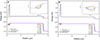 |
Figure 2 Simulated energy band diagrams of the nBn InGaAs structure for different Al compositions: (a) under equilibrium conditions and (b) under −150 mV reverse bias voltage. |
In Figure 2b, the 150 mV reverse bias confines Fermi level band bending within the large bandgap AlGaAs barrier, leaving the InGaAs absorption layer largely undepleted and thus effectively mitigating G-R dark current, in line with the core design principles of nBn photodetectors [19]. Therefore, an Al composition of 0.57 was adopted for subsequent electrical and optical simulations to ensure optimal device performance.
Following the determination of the optimal Al composition ratio for the nBn InGaAs structure, the influence of varying N-type doping concentrations within the AlGaAs barrier layer was examined Figure 3 presents the corresponding energy band diagrams under a 150 mV reverse bias for different doping levels. As simulated, increasing the N-type doping concentration leads to a higher VBO, whereas the undoped AlGaAs barrier exhibits the most favorable band alignment. Nevertheless, to ensure that the simulation results accurately reflect realistic device behavior and considering that background doping cannot be completely avoided during epitaxial growth the electrical simulations were performed assuming a maximum donor concentration of 1 × 1016 cm−3 in the AlGaAs barrier. This consideration ensures a closer correspondence between the simulated and experimentally achievable device performance [20].
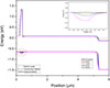 |
Figure 3 Energy band diagrams of the nBn InGaAs structure under a 150 mV reverse bias for different N-type doping concentrations in the AlGaAs barrier. |
Based on the optimized band alignment parameters, the device structure was defined as follows: 0.2 μm n−-In0.53Ga0.47As top n-contact layer (5 × 1017 cm−3), 0.1 μm n−-Al0.57Ga0.43As barrier layer (1 × 1016 cm−3), 5 μm n−-In0.53Ga0.47As absorber layer (5 × 1015 cm−3), 0.5 μm n+-InP bottom buffer n-contact layer (5 × 1018 cm−3) and 500 μm n+-InP substrate (5 × 1018 cm−3). The barrier thickness was determined according to the photocurrent versus potential curves presented in Figure 4 of Section 3. In addition, the absorber layer was designed to be relatively thick to achieve low capacitance, and lightly n-doped to further reduce the dark current [21].
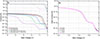 |
Figure 4 (a) Dark and photocurrent of the nBn-InGaAs structure with various barrier thickness, (b) dark current graph with different Al ratio. |
3 Results and discussion
In this section, all simulations were conducted at 300 K, with the lateral device active area set to 300 μm to reflect the geometry of commercial detectors, and all current values were normalized accordingly. Figure 4a shows the simulated current as a function of applied bias for different barrier thicknesses. Increasing the barrier thickness clearly reduces the dark current, but at the same time causes a relative decrease in photocurrent. Detailed analysis revealed that a barrier thickness of 100 nm provides the optimal balance: it maintains photocurrent levels comparable to those of thinner barriers while yielding nearly an order-of-magnitude reduction in dark current. In contrast, barrier layers thicker than 100 nm introduce a more pronounced photocurrent degradation, indicating that additional thickness imposes unnecessary transport resistance without a commensurate benefit in dark-current suppression. Thus, to optimize the trade-off between dark-current reduction and photo-response, the barrier thickness in the nBn-InGaAs structure was selected as 100 nm [6]. In Figure 4b, a sensitivity analysis was performed to evaluate the impact of band alignment uncertainties by varying the Al composition in the AlxGa1-xAs (x = 0.55–0.59) 100 nm barrier. The results show that variations in Al content do not produce significant changes in dark current characteristics, indicating a weak dependence of device performance on moderate fluctuations in CBO and VBO. These findings confirm the robustness of the proposed nBn-InGaAs design against variations in material composition and the associated band offset uncertainties.
As illustrated in Figure 4a, the nBn-InGaAs structure exhibits a significantly lower dark current compared to conventional mesa and planar InGaAs photodiodes [22, 23], while maintaining nearly the same photocurrent magnitude. Furthermore, the photocurrent characteristics presented in Figure 4a were obtained under back-illuminated operation with an incident optical power density of 0.1 W/cm2.
Figure 5 presents the decomposition of the dark current components as a function of reverse bias, providing insight into the dominant transport mechanisms in the proposed device. The total dark current (SUM) increases from approximately 3 × 10⁻¹⁴ A at 0 V to about 1 × 10⁻¹⁰ A at 1 V, exhibiting a gradual bias-dependent increase. Among the individual components, the SRH generation current dominates in the low-to-moderate bias range, indicating that generation–recombination processes are the primary contributor to the dark current [24, 25].
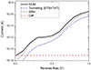 |
Figure 5 Dark current components as a function of reverse bias voltage at 300 K. |
In contrast, the tunneling current increases with reverse bias and becomes comparable to the SRH current at higher voltages, while remaining slightly lower overall, confirming that field-assisted leakage is effectively controlled by the barrier design. The diffusion current is nearly bias-independent and negligible in magnitude, suggesting minimal thermally driven carrier injection. Overall, these results demonstrate that the AlGaAs barrier effectively suppresses diffusion-related leakage, while the dark current is primarily governed by SRH generation at low bias and increasingly influenced by tunneling mechanisms at higher bias [26, 27]. These results confirm that the optimized barrier design effectively minimizes leakage pathways without compromising carrier collection efficiency, demonstrating the superior dark-current suppression capability of the nBn structure.
Following the analysis of the photocurrent characteristics, the simulated nBn-InGaAs structure was further evaluated in terms of its breakdown voltage and capacitance behavior, as presented in Figure 6. The results in Figure 6a show that the diode enters breakdown at approximately −82.5 V, primarily due to the combined effect of the thick absorber and barrier layers. This relatively high breakdown voltage highlights the structural robustness of the nBn configuration under strong reverse bias conditions and underscores its superior reliability compared to conventional pin InGaAs photodiodes [28], particularly in high-voltage and wide-dynamic-range applications. For comparison, conventional InGaAs pn photodiodes typically exhibit relatively low breakdown voltages due to the strong electric field concentration within the depletion region, which promotes early onset of avalanche multiplication through Impact Ionization. In such structures, the high doping gradients result in a narrow depletion width and consequently a large peak electric field, leading to breakdown at relatively low reverse biases. In contrast, nBn architectures eliminate the pn junction and instead rely on a unipolar barrier to control carrier transport. As a result, the electric field is more uniformly distributed across the device, significantly reducing the peak field intensity [29, 30].
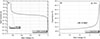 |
Figure 6 (a) Simulated I–V characteristics of the nBn-InGaAs structure and (b) C–V characteristics at 1 kHz. |
Figure 6b shows that the device exhibits a capacitance of approximately 9.2 pF at −5 V bias and 1 kHz frequency, which can be attributed to the presence of the thick absorber layer. Such a low capacitance not only minimizes noise but also enhances temporal response and dynamic range, resulting in improved signal fidelity for high-speed and low-noise infrared detection [31]. These findings demonstrate that, beyond its dark-current suppression capability, the nBn-InGaAs architecture combines electrical stability with excellent frequency response, confirming its potential for next-generation infrared photodetector technologies.
After evaluating the electrical characteristics, the photoresponsivity performance of the device was examined. Prior to responsivity analysis, the optical reflection behavior of the InP substrate was characterized, revealing that approximately 30% of the incident short-wavelength radiation is reflected from its surface. To enhance photon-to-electron conversion efficiency and improve overall responsivity, an anti-reflection (AR) coating was designed based on the reflectance formulation [32] in equation (1). Figure 7a compares the reflectance spectra of a bare InP surface with structures incorporating Si3N4 (140 nm) and SiO2 (150 nm) AR layers in the wavelength range of 0.8–1.7 μm. As illustrated, the AR-coated configuration significantly suppresses surface reflection, reducing it from nearly 30% to approximately 0.02% at 1.55 μm, which is expected to yield improved photocarrier generation and enhanced detector responsivity. Si3N4 and SiO2 were selected as AR materials due to their low extinction coefficients in the sub-2 μm band, making them well-suited for near-infrared photodetector applications [33]. (1)
(1) (2)
(2) (3)
(3) (4)
(4) (5)
(5) (6)
(6)
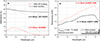 |
Figure 7 (a) Reflection and (b) responsivity graphs of the bare and AR-coated surfaces as a function of wavelength. |
To facilitate the definition of the reflectance expression in equation (6), the intermediate relations provided in equations (1)–(5) were utilized. Where n0 is denotes the refractive index of the incident medium, n1 the refractive index of the Si3N4 layer, n2 the refractive index of the SiO2 layer, and n3 the refractive index of the InP substrate. Similarly, t1 and t2 represent the physical thicknesses of the Si3N4 and SiO2 layers, respectively, while λ corresponds to the wavelength of the incident radiation.
In Figure 7b, the wavelength-dependent responsivity characteristics of the nBn-InGaAs photodetector are presented. To clearly demonstrate the influence of the anti-reflection coating on photo-response, the responsivity curves of both the AR-coated device and the bare surface are shown together. As observed, the application of the AR layer yields a substantial enhancement in photocarrier extraction efficiency: at the telecommunication wavelength of 1.55 μm [34], the responsivity increases by approximately 36%, improving from 0.60 to 0.82 A/W. This improvement is consistent with the reflectance reduction achieved through AR design and confirms that minimizing front-surface optical losses directly enhances the detector’s photon-to-electron conversion capability. In the numerical simulations performed in this study, the TCAD software provides external quantum efficiency (EQE) rather than responsivity as a direct output. Therefore, the EQE values were converted to responsivity using equation (7), enabling a direct comparison between the simulated and AR-enhanced device performance [35]. It should also be noted that the reported responsivity values correspond to conditions in which the nBn-InGaAs structure is illuminated from the backside under an incident optical power density of 0.01 W/cm2. Backside illumination ensures that the incident photons efficiently reach the absorbing InGaAs layer without encountering additional front-side metallization losses, thereby allowing a more accurate assessment of the intrinsic photo-response. Collectively, these results verify that integrating an appropriately engineered AR coating is an effective approach for maximizing optical coupling and elevating responsivity in nBn-type infrared photodetectors. (7)
(7)
where η is the EQE of the detector for a given wavelength, q is the electron charge, f is the frequency of the incident photons, and h is the Planck constant.
Figure 8 shows the responsivity variation with applied bias voltage, indicating that the proposed nBn design maintains high responsivity even at very low operating bias due to the minimized VBO and optimized barrier engineering. Notably, its performance approaches that of cutting-edge planar InGaAs detectors (Table 3), confirming the viability of the structure as a strong candidate for high-performance, low-power infrared photodetection.
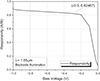 |
Figure 8 Bias voltage-dependent responsivity graph of nBn-InGaAs structure. |
Performance comparison of the proposed nBn photodetector with reported InGaAs-based photodetector.
To benchmark the proposed device, a comparison with previously reported InGaAs photodetectors is summarized in Table 3. The proposed nBn structure exhibits an ultra-low dark current of 1 pA at −0.3 V, which is significantly lower than reported nBn-InGaAs devices (0.9–8 nA) under similar bias conditions, corresponding to an improvement of several orders of magnitude. Compared to conventional pn junction, PIN diode, and pBin structures, which typically show dark currents in the range of 10–70 pA, the proposed device still demonstrates superior suppression.
The responsivity of 0.824 A/W at 1.55 μm is comparable to literature values, although slightly lower than the 1.08 A/W reported for pn-based devices. Overall, the results indicate that the proposed nBn design achieves an excellent trade-off between ultra-low dark current and competitive optical performance.
4 Conclusion
In this work, an InGaAs-based nBn photodetector incorporating an Al0.57Ga0.43As barrier layer was systematically designed and numerically analyzed using SILVACO ATLAS. Through detailed band alignment engineering, the optimal barrier composition was identified to achieve a near-zero valence band offset (ΔEv ≈ 35 meV) while maintaining a sufficiently large conduction band offset (ΔE𝚌 ≈ 1.26 eV). This configuration effectively enables barrier-free transport of minority carriers while strongly suppressing majority-carrier leakage, addressing one of the fundamental limitations of conventional InGaAs photodiodes. The optimized device demonstrates ultra-low dark current on the order of ~1 pA at low reverse bias (−0.3 V), representing orders-of-magnitude improvement compared to previously reported nBn-InGaAs structures. This significant reduction is primarily attributed to the suppression of Shockley–Read–Hall generation and diffusion-related leakage mechanisms, as confirmed by current component analysis. At higher biases, the controlled contribution of tunneling current further verifies the effectiveness of the barrier design in limiting field-assisted leakage. In addition to its low-noise performance, the proposed structure maintains competitive optical characteristics. By integrating a Si3N4/SiO2 anti-reflection coating, surface reflectance was reduced to nearly zero at 1.55 μm, resulting in a responsivity enhancement of approximately 36% (from 0.60 to 0.82 A/W). The device also exhibits low capacitance (~9.2 pF at −5 V) and a high breakdown voltage (−82.5 V), indicating its suitability for high-speed, low-noise, and wide dynamic range applications. Overall, this study demonstrates that precise control of barrier composition, doping, and layer thickness enables simultaneous optimization of electrical and optical performance in nBn architectures [39]. The presented design achieves an excellent trade-off between ultra-low dark current and high responsivity under low-bias operation, making it a strong candidate for next-generation short-wave infrared photodetectors operating under low-photon-flux and high-sensitivity conditions.
Funding
This research received no external funding.
Conflicts of interest
The authors declare that there are no conflicts of interest related to this article.
Data availability statement
The data is available from the corresponding author under reasonable request.
Author contribution statement
Ç. Tok was responsible for the conceptualization, design, simulation, formal analysis, investigation, methodology, resources, data curation, visualization, and writing of the original draft, as well as the review and editing of the manuscript.
M. Satılmış focused on the visualization, resources, methodology, investigation, and critical review of the manuscript.
H. Keleş handled the data curation, methodology, investigation, and re-editing of the manuscript.
F. Oğuz provided conceptualization, supervision, and contributed to the re-editing and design.
H. Sarı provided supervision and contributed to the conceptual framework.
E. Özbay oversaw the methodology, conceptual framework, and final manuscript approval.
References
- Rogalski A, Infrared detectors: an overview, Infrared Phys. Technol. 43(3–5), 187–210 (2002). https://doi.org/10.1016/S1350-4495(02)00140-8. [NASA ADS] [CrossRef] [Google Scholar]
- Thimsen E, Sadtler B, Berezin MY, Shortwave-infrared (SWIR) emitters for biological imaging: a review of challenges and opportunities, Nanophotonics 6(5), 1043–1054 (2017). https://doi.org/10.1515/nanoph-2017-0039. [Google Scholar]
- Schindler K, Wolf J, Krabbe A, Characterization of InGaAs-based cameras for astronomical applications using a new VIS-NIR-SWIR detector test bench, in Ground-based and Airborne Telescopes V, Vol. 9145 (SPIE, 2014). https://doi.org/10.1117/12.2057052. [Google Scholar]
- Satılmış M, et al. Investigation of sin x: H surface passivation impact on inasp/ingaas e-swir photodiodes, IEEE Sensors J 24(19), 29927–29936 (2024). https://doi.org/10.1109/JSEN.2024.3443747. [Google Scholar]
- Datta S, Joshi A, Rue J. Large-area InGaAs quad photoreceiver for laser interferometry space antenna, in Nanophotonics and Macrophotonics for Space Environments IV, Vol. 7817 (SPIE, 2010). https://doi.org/10.1117/12.861400. [Google Scholar]
- Uzgur F, Kocaman S, InGaAs nBn SWIR detector design with lattice-matched InAlGaAs barrier, Turk. J. Elect. Eng. Comput. Sci. 27(1), 1–10 (2019). https://doi.org/10.3906/elk-1802-197. [Google Scholar]
- Kopytko M., et al., Engineering the bandgap of unipolar HgCdTe-based nBn infrared photodetectors, J. Elect. Mater. 44 (1), 158–166 (2015). https://doi.org/10.1007/s11664-014-3511-9. [Google Scholar]
- Shi Q, et al., Progress on nBn infrared detectors, J. Infrared Millim. Waves 41, 1 (2022). https://doi.org/10.11972/j.issn.1001-9014.2022.01.010. [Google Scholar]
- Walker AW, Denhoff MW, Minority carrier diffusion lengths and mobilities in low-doped n-InGaAs for focal plane array applications, in Infrared Technology and Applications XLIII, Vol. 10177 (SPIE, 2017). https://doi.org/10.1117/12.2258616. [Google Scholar]
- Tok Ç, et al., Design and simulation of SWIR nBn-InGaAs photodetector with AlGaAs barrier, in EPJ Web of Conferences, Vol. 335 (EDP Sciences, 2025). https://doi.org/10.1051/epjconf/202533511002. [Google Scholar]
- Şahin A, et al., A numerical design for SWIR/eSWIR dual-band operation with InGaAs nBn structures, in Quantum Sensing and Nano Electronics and Photonics XVIII, Vol. 12009 (SPIE, 2022). https://doi.org/10.1117/12.2610186. [Google Scholar]
- Liang Y, et al., InP-based GaAsSb/AlGaAsSb/T2SL barrier-type low-bias tunable dual-band NIR/eSWIR photodetectors, Opt. Express 32(13), 23822–23830 (2024). https://doi.org/10.1364/oe.528762. [Google Scholar]
- Xie R, et al., Extended short-wave infrared barrier structure focal plane array based on InGaAs/GaAsSb type-ii superlattices, J. Lightwave Technol. 43(5), 2271–2276 (2025). https://doi.org/10.1109/JLT.2024.3491901. [Google Scholar]
- Silvaco I, ATLAS User’s Manual: A 2D Numerical Device Simulator (2016). [Google Scholar]
- Şahin A, et al., Dual-band InGaAs nBn photodetectors at 2 μm, Appl. Phys. Lett., 120, 9 (2022). https://doi.org/10.1063/5.0080950. [Google Scholar]
- Khamis MA, et al., Effect of multiplication and absorption layers width on avalanche multiplication gain in InGaAs/InP avalanche photodiode, Int. J. Eng. Technol. 7.4.35, 559–563 (2018). [Google Scholar]
- Salem MS, et al., Performance optimization of the InGaP/GaAs dual-junction solar cell using SILVACO TCAD, Int. J. Photoenergy (2021) (1), 8842975 2021. https://doi.org/10.1155/2021/8842975. [Google Scholar]
- Liu S, et al., Investigation of the growth temperature of AlGaAs barrier layer on optical and crystal quality of InGaAs/AlGaAs multi-quantum wells and AlGaAs single layer grown by molecular beam epitaxy (MBE), Mater. Sci. Semicond. Process. 187, 109140 (2025). https://doi.org/10.1016/j.mssp.2024.109140. [Google Scholar]
- Maimon S, Wicks GW, nBn detector, an infrared detector with reduced dark current and higher operating temperature, Appl. Phys. Lett. 89, 15 (2006). https://doi.org/10.1063/1.2360235. [Google Scholar]
- He Z, et al., The effect of unintentional carbon incorporation on the electrical properties of AlGaAs grown by MOCVD, Opt. Mater. 108, 110227 (2020). https://doi.org/10.1016/j.optmat.2020.110227. [Google Scholar]
- Liu H, et al., Design and fabrication of high performance InGaAs near infrared photodetector, Nanomaterials 13(21), 2895 (2023). https://doi.org/10.3390/nano13212895 [Google Scholar]
- Koronnov AA, et al., InGaAs/InP PIN photodiode for optical receivers in pulsed-laser range finding systems, Bull. Lebedev Phys. Inst. 52(Suppl 1), S106–S112 (2025). https://doi.org/10.3103/S1068335625600263. [Google Scholar]
- Andreev DS, et al., Investigation of planar photodiodes of a focal plane array based on a heteroepitaxial InGaAs/InP structure, J. Commun. Technol. Electr. 61(10), 1220–1225 (2016). https://doi.org/10.1134/S1064226916100028. [Google Scholar]
- Savich GR, et al., Dark current filtering in unipolar barrier infrared detectors, Appl. Phys. Lett. 99, 12 (2011). https://doi.org/10.1063/1.3643515. [Google Scholar]
- Savich GR, et al., Use of unipolar barriers to block dark currents in infrared detectors, in Infrared Technology and Applications XXXVII, Vol. 8012 (SPIE, 2011). https://doi.org/10.1117/12.884075. [Google Scholar]
- Gravrand O, Boulard F, Ferron A, Ballet P, Hassis W, A new nBn IR detection concept using HgCdTe material. J. Elect. Mater. 44(9), 3069–3075 (2015). https://doi.org/10.1007/s11664-015-3821-6. [Google Scholar]
- Thi L, Yen YK, Mori N, A comparison of mechanisms for improving dark current characteristics in barrier infrared photodetectors, Jpn. J. Appl. Phys. 59(4), 044005 (2020). https://doi.org/10.35848/1347-4065/ab7e77. [Google Scholar]
- Bauer JG, Trommer R, Long-term operation of planar InGaAs/InP pin photodiodes, IEEE Trans. Electron Devices 35(12), 2349–2354 (2002). https://doi.org/10.1109/16.8813. [Google Scholar]
- Zhang Q, et al., Tuning Ga2O3-based avalanche photodetectors performance through barrier layer thickness optimization, Mater. Design 239, 112823 (2024). https://doi.org/10.1016/j.matdes.2024.112823. [Google Scholar]
- Zhang Q, et al., Enhanced gain and detectivity of unipolar barrier solar blind avalanche photodetector via lattice and band engineering, Nat. Commun. 14(1), 418 (2023). https://doi.org/10.1038/s41467-023-36117-8. [Google Scholar]
- Bucsa I, et al., Large area, low capacitance InGaAs PINs, in Physics and Simulation of Optoelectronic Devices XXIX, Vol. 11680 (SPIE, 2021). https://doi.org/10.1117/12.2578824. [Google Scholar]
- Moys BA The theory of double-layer antireflection coatings, Thin Solid Films 21(1), 145–157 (1974). https://doi.org/10.1016/0040-6090(74)90097-2. [Google Scholar]
- Oh G, et al., Broadband antireflective coatings for high efficiency InGaP/GaAs/InGaAsP/InGaAs multi-junction solar cells, Solar Energy Mater. Solar Cells 207, 110359 (2020). https://doi.org/10.1016/j.solmat.2019.110359. [Google Scholar]
- Milostnaya I, et al., Superconducting single-photon detectors designed for operation at 1.55-μm telecommunication wavelength, J. Phys. Conf. Ser. 43(1) IOP Publishing (2006). https://doi.org/10.1088/1742-6596/43/1/326. [Google Scholar]
- Sze SM, Li Y, Kwok KNg, Physics of Semiconductor Devices (John Wiley & Sons, 2021). [Google Scholar]
- Klem JF, et al., Mesa-isolated InGaAs photodetectors with low dark current, Appl. Phys. Lett. 95(3), (2009) https://doi.org/10.1063/1.3184807. [Google Scholar]
- Dolas MH, et al.. Low dark current diffusion limited planar type InGaAs photodetectors, in Infrared Sensors, Devices, and Applications IX, Vol. 11129 (SPIE, 2019). https://doi.org/10.1117/12.2528666. [Google Scholar]
- Chang S-H, et al., Ultra high performance planar InGaAs PIN photodiodes for high speed optical fiber communication, Sens. Actuat. A Phys. 133(1), 9–12 (2007). https://doi.org/10.1016/j.sna.2006.04.023. [Google Scholar]
- Martyniuk P, Rogalski A, HOT infrared photodetectors, Opto-Elect. Rev. 21(2), 239–257 (2013). https://doi.org/10.2478/s11772-013-0090-x. [Google Scholar]
All Tables
Physical models used in SILVACO ATLAS simulation for nBn InGaAs photodetector design.
Performance comparison of the proposed nBn photodetector with reported InGaAs-based photodetector.
All Figures
|
Figure 1 (a) Planar design, and (b) band diagram of nBn structure. |
| In the text | |
|
Figure 2 Simulated energy band diagrams of the nBn InGaAs structure for different Al compositions: (a) under equilibrium conditions and (b) under −150 mV reverse bias voltage. |
| In the text | |
|
Figure 3 Energy band diagrams of the nBn InGaAs structure under a 150 mV reverse bias for different N-type doping concentrations in the AlGaAs barrier. |
| In the text | |
|
Figure 4 (a) Dark and photocurrent of the nBn-InGaAs structure with various barrier thickness, (b) dark current graph with different Al ratio. |
| In the text | |
|
Figure 5 Dark current components as a function of reverse bias voltage at 300 K. |
| In the text | |
|
Figure 6 (a) Simulated I–V characteristics of the nBn-InGaAs structure and (b) C–V characteristics at 1 kHz. |
| In the text | |
|
Figure 7 (a) Reflection and (b) responsivity graphs of the bare and AR-coated surfaces as a function of wavelength. |
| In the text | |
|
Figure 8 Bias voltage-dependent responsivity graph of nBn-InGaAs structure. |
| In the text | |
Current usage metrics show cumulative count of Article Views (full-text article views including HTML views, PDF and ePub downloads, according to the available data) and Abstracts Views on Vision4Press platform.
Data correspond to usage on the plateform after 2015. The current usage metrics is available 48-96 hours after online publication and is updated daily on week days.
Initial download of the metrics may take a while.