| Issue |
J. Eur. Opt. Society-Rapid Publ.
Volume 21, Number 1, 2025
|
|
|---|---|---|
| Article Number | 28 | |
| Number of page(s) | 6 | |
| DOI | https://doi.org/10.1051/jeos/2025022 | |
| Published online | 27 June 2025 | |
Research Article
Plasmonic characteristics of magnetized plasma–graphene-magnetized plasma–perfect magnetic conductor planar waveguides
1
Department of Physics, University of Agriculture, Faisalabad, Pakistan
2
Department of Electrical Engineering, King Saud University, Riyadh, Saudi Arabia
3
School of Materials Science and Engineering, Zhengzhou University, Zhengzhou 450001, PR China
* Corresponding authors: This email address is being protected from spambots. You need JavaScript enabled to view it.
; This email address is being protected from spambots. You need JavaScript enabled to view it.
Received:
28
March
2025
Accepted:
24
April
2025
Abstract
This manuscript explores the novel characteristics of surface plasmon polaritons (SPPs) in the terahertz (THz) frequency region by numerically investigating the magnetized plasma–graphene-magnetized plasma–perfect magnetic conductor (PMC) planar interface. Substrates are assumed to be PMCs. The dispersion equations for the field components are derived, and the Kubo formula is utilized for the physical modeling of graphene conductivity. The numerical results show that the plots of effective mode index, propagation length, and phase velocity can be varied by adjusting the chemical potential, number of graphene layers, and tensorial permittivity parameters of the magnetized plasma medium (i.e., plasma frequency and cyclotron frequency). Furthermore, the cutoff frequency for the proposed waveguide structure is analyzed.
Key words: Plasmonics / Graphene / Magnetized Plasma / Waveguide / Perfect magnetic conductor
© The Author(s), published by EDP Sciences, 2025
 This is an Open Access article distributed under the terms of the Creative Commons Attribution License (https://creativecommons.org/licenses/by/4.0), which permits unrestricted use, distribution, and reproduction in any medium, provided the original work is properly cited.
Introduction
Like electronics, optics and photonics are extremely efficient technologies that can be used in a wide variety of industries across various fields. Although information processing is still based on electronic transistors and microchips, photonic alternatives are increasingly being incorporated into information technology. The use of photonic devices and technologies can be found in a number of fields, such as communications, information processing, manufacturing, biomedical, sensing, defense, and security. With photonics as a means for transmitting and processing signals, power consumption can be reduced, operation speed can be increased, and bandwidth can be widened [1]. However, many challenges are associated with photonic devices, including the need for high levels of precision [2]. Furthermore, unlike electronic devices, which are based on transistors, photonic devices are not designed on the basis of a base unit. To overcome such limitations, plasmonic devices have been proposed as a replacement for photonic devices [3]. In the optics community, the nanophotonics and plasmonics fields have often been combined because of their capability of operating on subwavelength scales and integrating with electronics. In recent years, the field of plasmonics has drawn considerable attention due to the ability to confine electromagnetic (EM) waves to device sizes that are compatible with electronics [4]. In plasmonics, a surface wave is generated when an EM wave is coupled to oscillations of a delocalized electron in metal at a dielectric metal interface, which are known as surface plasmon polaritons (SPPs). In metal, these waves are confined to tens of nanometers, which allows plasmonic devices to be designed on this scale and integrated with electronic devices [5]. In this context, different authors have used various optical materials for the propagation of metal-based SPPs [6–11]. However, as with any other technology, there are challenges associated with plasmonics. At terahertz (THz) frequencies, metal shows propagation losses. A major disadvantage of plasmonic waveguides is the extremely high propagation losses, particularly when the mode of confinement is on a subwavelength level [12]. SPP modes are subject to this fundamental limitation: stronger SPP confinement pushes the field closer to the metal, which results in higher propagation losses. Optics researchers are exploring new optical materials to overcome these challenges.
Graphene SPPs offer unique research opportunities for scientists and possess exceptional electrical and optical properties [13, 14]. Compared to metal dielectric SPP waves, graphene SPP waves exhibit a very strong confinement mode and low propagation loss [15, 16]. One of graphene’s most notable properties is its zero-bandgap structure, which distinguishes it from other naturally occurring materials, since graphene electrons behave like massless fermions, which is very promising for making compact nanophotonic devices. Additionally, graphene’s surface conductivity can be modified by altering the chemical potential, relaxation time, and frequency of its EM waves. The electrical properties of graphene are strongly influenced by these parameters, making it an extremely versatile material with a wide range of applications in a variety of fields such as electronics and optoelectronics [17, 18]. Furthermore, the carrier concentration in graphene is controlled by electrical gating, and this control is extremely influential over the electronic characteristics of graphene [19].
Perfect magnetic conductor (PMC) waveguides are becoming increasingly important for the analysis of EM wave propagation. Several researchers have conducted research relevant to PMC boundary conditions [20–23]. It has been reported that PMC surfaces have extremely high surface impedance within certain frequency ranges. In addition, PMC surfaces reflect EM waves without changing the electric field phase unlike perfect electrical conductor surfaces [24]. The boundary conditions that exist at the surface of a PMC are as follows [20, 22, 25]: (1)
(1)
 (2)where
n represents the unit vector normal to the PMC surface.
(2)where
n represents the unit vector normal to the PMC surface.
Mathematical formulation
Consider the planar waveguide filled with graphene, surrounded by magnetized plasma, and with a PMC as the substrate shown in Figure 1.
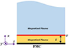 |
Figure 1 Configuration of magnetized plasma–graphene–magnetized plasma–PMC planar waveguide. |
For the magnetized plasma, the constitutive relations are given as [26]: (3)
(3)
 (4)
(4)
 is given below:
![Mathematical equation: $$ [\stackrel{=}{\epsilon }]=\left[\begin{array}{ccc}{\epsilon }_1& -j{\epsilon }_2& 0\\ j{\epsilon }_2& {\epsilon }_1& 0\\ 0& 0& {\epsilon }_3\end{array}\right]. $$](/articles/jeos/full_html/2025/01/jeos20250026/jeos20250026-eq6.gif) (5)
ε1
, ε2, and ε3 are permittivity tensor values, as reported in [27]. In terms of Hz and Ez, the magnetized plasma wave equation can be expressed as follows [28]:
(5)
ε1
, ε2, and ε3 are permittivity tensor values, as reported in [27]. In terms of Hz and Ez, the magnetized plasma wave equation can be expressed as follows [28]:![Mathematical equation: $$ \left[\begin{array}{c}{\nabla }^2{E}_z\\ {\nabla }^2{H}_z\end{array}\right]+\left[\begin{array}{cc}{s}_1& {{js}}_2\\ {{js}}_3& {s}_4\end{array}\right]\left[\begin{array}{c}{E}_z\\ {H}_z\end{array}\right]=0, $$](/articles/jeos/full_html/2025/01/jeos20250026/jeos20250026-eq7.gif) (6)where
(6)where (7)
(7)
 (8)
(8)
 (9)
(9)
 (10)
(10)
 (11)where the eigenvalues of magnetized plasma are [29]:
 (12)
(12)
 (13)
(13)
The EM fields associated with the magnetized plasma media are as follows [29]: (14)
(14)
 (15)
(15)
 (16)
(16)
 (17)where
  ,
,  ,
,  ,
,  ,
,  and
and  are unknown constants. The remaining EM field components can be obtained from [30]. The boundary conditions applied at the magnetized plasma–graphene–magnetized plasma–PMC interface are given below:
![Mathematical equation: $$ \hat{x}\times \left[{H}_1-{H}_2\right]={\sigma E}, $$](/articles/jeos/full_html/2025/01/jeos20250026/jeos20250026-eq25.gif) (18)
(18)
![Mathematical equation: $$ \hat{x}\times \left[{E}_1-{E}_2\right]=0, $$](/articles/jeos/full_html/2025/01/jeos20250026/jeos20250026-eq26.gif) (19)where σ is the graphene conductivity as reported in [31]: By applying Equations (18) and (19) to the proposed waveguide structure, the following matrix is obtained:
(19)where σ is the graphene conductivity as reported in [31]: By applying Equations (18) and (19) to the proposed waveguide structure, the following matrix is obtained:![Mathematical equation: $$ \left[\begin{array}{ccc}\begin{array}{c}{b}_{11}\\ {b}_{21}\\ \begin{array}{c}{b}_{31}\\ {b}_{41}\\ \begin{array}{c}{b}_{51}\\ {b}_{61}\end{array}\end{array}\end{array}& \begin{array}{c}{b}_{12}\\ {b}_{22}\\ \begin{array}{c}{b}_{32}\\ {b}_{42}\\ \begin{array}{c}{b}_{52}\\ {b}_{62}\end{array}\end{array}\end{array}& \begin{array}{ccc}\begin{array}{c}{b}_{13}\\ {b}_{23}\\ \begin{array}{c}{b}_{33}\\ {b}_{43}\\ \begin{array}{c}{b}_{53}\\ {b}_{63}\end{array}\end{array}\end{array}& \begin{array}{c}{b}_{14}\\ {b}_{24}\\ \begin{array}{c}{b}_{34}\\ {b}_{44}\\ \begin{array}{c}{b}_{54}\\ {b}_{64}\end{array}\end{array}\end{array}& \begin{array}{cc}\begin{array}{c}{b}_{15}\\ {b}_{25}\\ \begin{array}{c}{b}_{35}\\ {b}_{45}\\ \begin{array}{c}{b}_{55}\\ {b}_{65}\end{array}\end{array}\end{array}& \begin{array}{c}{b}_{16}\\ {b}_{26}\\ \begin{array}{c}{b}_{36}\\ {b}_{46}\\ \begin{array}{c}{b}_{56}\\ {b}_{66}\end{array}\end{array}\end{array}\end{array}\end{array}\end{array}\right]\left[\begin{array}{c}{c}_1\\ {c}_2\\ \begin{array}{c}{c}_3\\ {c}_4\\ \begin{array}{c}{c}_5\\ {c}_6\end{array}\end{array}\end{array}\right]\enspace =0.\enspace $$](/articles/jeos/full_html/2025/01/jeos20250026/jeos20250026-eq27.gif) (20)
(20)
Here,
b11 = 0, b12 = −j(f + bα1)u1 − M(b − dα1)u1, b13 = 0, b14 = −j(f + bα2) u2 − M(b − dα2)u2, b15 = 0, b16 = 0, b21 = M + jα1, b22 = 0, b23 = M + jα2, b24 = 0, b25 = 0, b24 = 0, b31 = −j(f + bα1)u1 sin[tu1], b32 = j(f + bα1)cos[tu1]u1, b33 = −j(f + bα2)u2 sin[tu2], b34 = j(f + bα2)u2 cos[tu2],  ,
,  , b41 = −jcos[tu1]α1, b42 = −jsin[tu1] α1, b43 = −jcos[tu2]α2, b44 = −jsin[tu2]α2,
  ,
,  , b51 = −(b − dα1)u1 sin[tu1], b52 = cos[tu1](b − dα1)u1, b53 = −sin[tu2]u2 (b − dα2), b54 = cos[tu2]u2 (b − dα2),
  ,
,  , b61 = −cos[tu1], b62 = −sin[tu1], b63 = −cos[tu2], b64 = −sin[tu2],
  ,
,  .
.
Results
This section numerically examines dispersion equation (20) for a sandwiched structure at the magnetized plasma–graphene–magnetized plasma–PMC planar interface to explore the novel SPPs in the THz frequency region. Figure 2a illustrates the relationship between the effective mode index and propagation frequency for different chemical potentials. In graphene, the optical conductivity varies with the chemical potential. In response to an increase in chemical potential, the real part of optical conductivity increases, thereby resulting in a stronger interaction with the EM field. As a result, the optical mode becomes more confined within or near the graphene layer, resulting in a higher effective mode index. Figure 2 also shows that as the magnitude of the chemical potential increases, the dispersion curves shift from the low-frequency to the high-frequency region, and the propagation frequency decreases. It is observed that the slope of the dispersion curve is smaller for lower chemical potential values. Furthermore, at lower propagation frequencies, the dispersion curves exhibit less significant behaviors. The dependence of the effective mode index on the number of graphene layers versus the propagation frequency is analyzed in Figure 2b. It is clearly seen that the effective mode index increases but the cutoff frequency decreases for multilayer graphene. An increase in the number of graphene layers results in an increase in the overall thickness of the waveguide structure. Moreover, the multilayer graphene structure interacts more strongly with the EM field than the single-layer graphene structure. In addition, the multilayers enhance graphene’s ability to support SPPs or guided modes, increasing the effective mode index. The dependence of the effective mode index on the plasma frequency and cyclotron frequency versus the propagation frequency is analyzed in Figures 3a and 3b, respectively. According to Figure 3a, the cutoff frequency and effective mode index increase with the plasma frequency. An increase in plasma frequency results in an increase in electron density. As a result, the EM wave and the plasma are more strongly coupled.
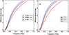 |
Figure 2 Dependence of effective mode index on chemical potential and number of graphene layers at τ = 50 ps, t = 100 nm and μ = 0.2 eV. |
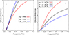 |
Figure 3 Dependence of effective mode index on plasma frequency and cyclotron frequency at τ = 50 ps, t = 100 nm, ωc = 3 × 10¹¹ Hz and ωp = 2 THz. |
Increasing the effective mode index signifies a decrease in the phase velocity of the wave, thereby indicating stronger confinement and slower propagation of the wave through the magnetized plasma. Furthermore, the slope of the dispersion curve decreases with the plasma frequency. Figure 3b illustrates the dependence of the effective mode index on the cyclotron frequency versus the propagation frequency. As the cyclotron frequency increases, the effective mode index decreases, but the dispersion curves start shifting toward the high-propagation-frequency region. When the cyclotron frequency increases, the phase velocity of the EM wave increases due to the influence of the magnetic field. The plasma permittivity tensor components change due to this effect. An increase in the phase velocity leads to a decrease in the effective mode index. It is concluded that using the plasma frequency and cyclotron frequency of the magnetized plasma medium for the proposed waveguide structure can enable the plasmonic community to investigate new phenomena, develop advanced materials, and design innovative devices.
To better understand the SPP properties for the proposed waveguide structure, the propagation length and phase velocity are shown in Figures 4 and 5, respectively. Figure 4a depicts the dependence of the propagation length on the plasma frequency in the THz-propagation-frequency region. The propagation frequency increases with the plasma frequency. It is worth noting that in contrast to Figure 2a, the slope of variation decreases with the plasma frequency. Furthermore, a higher cutoff frequency is achieved at the highest plasma frequency (i.e., ωp = 4 THz). Figure 4b plots the variation in propagation length with cyclotron frequency. The cutoff frequency increases with the cyclotron frequency. Furthermore, increasing the cyclotron frequency causes the propagation frequency band to narrow. Figures 5a and 5b illustrate the variation in phase velocity under varying chemical potentials and plasma frequencies. Figure 5a clearly shows that the propagation frequency and bandgap decrease when the chemical potential is increased. Moreover, at higher propagation frequencies, the dispersion curves demonstrate non-significant behaviors, which is of no practical significance in the field of plasmonics. Figure 5b illustrates the dependence of the phase velocity on the propagation frequency for different plasma frequencies. It is evident that the propagation frequency and phase velocity can be varied by substantially varying the plasma frequency of the magnetized plasma medium.
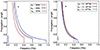 |
Figure 4 Dependence of propagation length on plasma frequency and cyclotron frequency τ = 50 ps, t = 100 nm and μ = 0.2 eV. |
 |
Figure 5 Dependence of phase velocity on chemical potential and plasma frequency τ = 50 ps, t = 100 nm and ωc = 3 × 10¹¹ Hz. |
Concluding remarks
This research examined the generation of tunable EM surface waves at magnetized plasma–graphene–magnetized plasma–PMC planar interfaces. We demonstrated that the propagation features associated with surface waves (i.e., effective mode index, propagation frequency, and phase velocity) are strongly dependent on magnetized plasma features (i.e., plasma frequency and cyclotron frequency) and graphene features. We also studied the propagation frequency of the proposed waveguide structure and found that propagation frequency fluctuations offer additional flexibility to modify its plasmonic properties. It is believed that the proposed scheme could provide a useful approach for the design of high-performance THz devices.
Acknowledgments
The authors would like to thank King Saud University, Riyadh, Saudi Arabia for Supporting through Ongoing Research Funding Program (ORF-2025-416).
Funding
This work was supported through the Ongoing Research Funding Program (ORF-2025-416). King Saud University, Riyadh, Saudi Arabia.
Conflicts of interest
The authors declare that they have no known competing financial interests or personal relationships that could have appeared to influence the work reported in this paper.
Data availability statement
Detail about data has been provided in the article.
Author contribution statement
M Umair wrote main manuscript and derived analytical expressions. A. Ghaffar and Majeed A. S. Alkanhal edited the manuscript and reviewed the numerical analysis. Y. Khan, M.U. Shahid and M. Amir. Ali developed methodology in the given study. All authors reviewed the manuscript before submission.
References
- National Research Council, Division on Engineering, Physical Sciences, National Materials, Manufacturing Board, Committee on Harnessing Light, et al., Optics and photonics: Essential technologies for our nation (National Academies Press, 2013). [Google Scholar]
- Hochberg M, Harris NC, Ding R, Zhang Y, Novack A, Xuan Z, et al., Silicon photonics: the next fabless semiconductor industry, IEEE Solid-State Circuits Mag. 5(1), 48–58 (2013). [Google Scholar]
- Zia R, Schuller JA, Chandran A, Brongersma ML, Plasmonics: the next chip-scale technology, Mater. Today 9(7–8), 20–27 (2006). [Google Scholar]
- Tong L, Wei H, Xu H., Fundamentals of Plasmonics. Nanophotonics (Jenny Stanford Publishing, 2017), pp. 1–20. [Google Scholar]
- Ozbay E, Plasmonics: merging photonics and electronics at nanoscale dimensions, Science 311(5758), 189–193 (2006). [NASA ADS] [CrossRef] [Google Scholar]
- Bousbih R, Soliman M, Jafar N, Jabir M, Majdi H, Alshomrany A, et al., Generation of Surface Plasmon Polaritons (SPPs) at chiroplasma-metal interface, Plasmonics, 1–6. [Google Scholar]
- Iftikhar M, Raza A, Alkhouri A, Ibrahim S, Obaidullah A, Mahal A, et al., Numerical investigations of SPPs at chiroferrite-metal interface. Plasmonics, 1–6 (2024). [Google Scholar]
- Mi G, Van V, Characteristics of surface plasmon polaritons at a chiral–metal interface, Opt. Lett. 39(7), 2028–2031 (2014). [Google Scholar]
- Polo JA, Jr., Lakhtakia A, On the surface plasmon polariton wave at the planar interface of a metal and a chiral sculptured thin film, Proc. R. Soc A Math. Phys. Eng. Sci. 465(2101), 87–107 (2009). [Google Scholar]
- Zhang Q, Li J, Characteristics of surface plasmon polaritons in a dielectrically chiral-metal-chiral waveguiding structure, Opt. Lett. 41(14), 3241–3244 (2016). [Google Scholar]
- Zhang Q, Li J, Liu X, Gelmecha DJ, Dispersion, propagation, and transverse spin of surface plasmon polaritons in a metal-chiral-metal waveguide, Appl. Phys. Lett. 110(16), (2017). [Google Scholar]
- Ebbesen TW, Genet C, Bozhevolnyi SI, Surface-plasmon circuitry, Phys. Today 61(5), 44–50 (2008). [Google Scholar]
- Mahal A, Abdulghani HH, Khamis RA, Asiri YM, Amin MA, Jabir MS, et al., Characteristics of photon–plasmon coupling in uniaxial chiral filled slab waveguide bounded by graphene layers, Plasmonics, 1–8 (2024). [Google Scholar]
- Bani-Fwaz MZ, Bousbih R, Khamis RA, Soliman MS, Jabir MS, Majdi H, et al., Graphene-Loaded Surface Plasmon Polariton (SPP) waveguide surrounded by Uniaxial Chiral (UAC) and plasma layers, Plasmonics, 1–8 (2024). [Google Scholar]
- Lu WB, Zhu W, Xu HJ, Ni ZH, Dong ZG, Cui TJ, Flexible transformation plasmonics using graphene, Opt. Exp. 21(9), 10475–10482 (2013). [Google Scholar]
- Yaqoob M, Ghaffar A, Alkanhal M, Ur Rehman S, Razzaz F, Hybrid surface plasmon polariton wave generation and modulation by Chiral-Graphene-Metal (CGM) structure, Sci. Rep. 8(1), 1–9 (2018). [Google Scholar]
- Roumi B, Abdi-Ghaleh R, Akkus H, Single-frequency into dual-frequency absorption switch based on a one-dimensional photonic crystal containing graphene and vanadium dioxide layers, Photon. Nanostruct. Fundament. Appl. 53, 101111 (2023). [Google Scholar]
- Roumi B, Abdi-Ghaleh R, Madani A, Optical phase shift changes of 2D graphene on a substrate, Eur.Phys. J. Plus 134(7), 329 (2019). [Google Scholar]
- Saeed M, Ghaffar A, Rehman SU, Naz MY, Shukrullah S, Naqvi QA, Graphene-based plasmonic waveguides: a mini review, Plasmonics 17(3), 901–911 (2022). [Google Scholar]
- Edery A, Marachevsky V, Perfect magnetic conductor Casimir piston in d+1 dimensions, Phys. Rev. D Particles, Fields, Gravitation, and Cosmology 78(2), 025021 (2008). [Google Scholar]
- Feresidis AP, Goussetis G, Wang S, Vardaxoglou JC, Artificial magnetic conductor surfaces and their application to low-profile high-gain planar antennas, IEEE Trans. Antennas Propag. 53(1), 209–215 (2005). [Google Scholar]
- Ghaffar A, Alkanhal MA, Propagation through chiroplasma waveguide using perfect magnetic conductor boundary conditions, Can. J. Phys. 93(12), 1460–1465 (2015). [Google Scholar]
- Liu L-l, Li Z, Gu C-Q, Ning P-P, Xu B-Z, Niu Z-Y, et al., A corrugated perfect magnetic conductor surface supporting spoof surface magnon polaritons, Opt. Exp. 22(9), 10675–10681 (2014). [Google Scholar]
- Sohn J, Kim KY, Tae H-S, Lee H, Comparative study on various artficial magnetic conductors for low-profile antenna, Prog. Electromagn. Res. 61, 27–37 (2006). [Google Scholar]
- Baqir M, Choudhury P, On the energy flux through a uniaxial chiral metamaterial made circular waveguide under PMC boundary, J. Electromagn. Waves Appl 26(16), 2165–2175 (2012). [Google Scholar]
- Umair M, Azam M, Alkanhal MA, Ghaffar A, Aladadi YT, Khan Y, Characteristics of surface plasmon polaritons in magnetized plasma film walled by two graphene layers, J. Nanoelectron. Optoelectron. 15(5), 574–579 (2020). [Google Scholar]
- Shahid MU, Ghaffar A, Alkanhal MA, Khan Y, Propagation of electromagnetic waves in graphene-wrapped cylindrical waveguides filled with magnetized plasma, Optik 244, 167566 (2021). [Google Scholar]
- Ali M, Ghaffar A, Alkanhal MA, Khan Y, Study of hybrid surface Plasmon modes in metallic circular waveguide filled with magnetized plasma, Waves Random Complex Media 32(1), 449–462 (2022). [Google Scholar]
- Azama M, Ghaffara A, Jamila Y, Bhattib H, Hybrid surface plasmon polariton (SPPs) modes between metal and anisotropic plasma interface, J. Ovonic Res. 17(6), 509–517 (2021). [Google Scholar]
- Gong J, Electromagnetic wave propagation in a chiroplasma-filled waveguide, J. Plasma Phys. 62(1), 87–94 (1999). [Google Scholar]
- Yaqoob MZ, Ghaffar A, Alkanhal M, Rehman SU, Characteristics of light–plasmon coupling on chiral–graphene interface, J. Opt. Soc. Am. B 36(1), 90–95 (2018). [Google Scholar]
All Figures
|
Figure 1 Configuration of magnetized plasma–graphene–magnetized plasma–PMC planar waveguide. |
| In the text | |
|
Figure 2 Dependence of effective mode index on chemical potential and number of graphene layers at τ = 50 ps, t = 100 nm and μ = 0.2 eV. |
| In the text | |
|
Figure 3 Dependence of effective mode index on plasma frequency and cyclotron frequency at τ = 50 ps, t = 100 nm, ωc = 3 × 10¹¹ Hz and ωp = 2 THz. |
| In the text | |
|
Figure 4 Dependence of propagation length on plasma frequency and cyclotron frequency τ = 50 ps, t = 100 nm and μ = 0.2 eV. |
| In the text | |
|
Figure 5 Dependence of phase velocity on chemical potential and plasma frequency τ = 50 ps, t = 100 nm and ωc = 3 × 10¹¹ Hz. |
| In the text | |
Current usage metrics show cumulative count of Article Views (full-text article views including HTML views, PDF and ePub downloads, according to the available data) and Abstracts Views on Vision4Press platform.
Data correspond to usage on the plateform after 2015. The current usage metrics is available 48-96 hours after online publication and is updated daily on week days.
Initial download of the metrics may take a while.