| Issue |
J. Eur. Opt. Society-Rapid Publ.
Volume 22, Number 1, 2026
EOSAM 2025
|
|
|---|---|---|
| Article Number | 28 | |
| Number of page(s) | 7 | |
| DOI | https://doi.org/10.1051/jeos/2026022 | |
| Published online | 24 April 2026 | |
Research Article
Enhancing fluorescence of low quantum yield fluorophores with plasmonic metasurfaces
National Institute for Research and Development in Microtechnology – IMT Bucharest, 126A, Erou Iancu Nicolae Street, 077190, Voluntari, Ilfov, Romania
* Corresponding author: This email address is being protected from spambots. You need JavaScript enabled to view it.
Received:
30
January
2026
Accepted:
4
March
2026
Abstract
Metasurfaces represent an innovative category of optical surfaces that can be engineered to exhibit distinctive properties that are not observed in conventional materials. It has been demonstrated that these structures exhibit robust light-matter interactions at the nanoscale, which renders them a promising solution for enhancing the sensitivity of various biomedical sensing technologies. This work presents a versatile approach for enhancing the broadband spectral emission of various fluorophores. The approach involves developing large-area, lithography-free plasmonic platforms without tailoring the geometry of the metasurface to a specific chromophore. The investigation encompasses the fluorescence behaviour of low quantum yields fluorophores such as Crystal Violet, Nile Red, and Rose Bengal, dispersed in ethanol solutions and coated onto the metallic arrays with random configuration. The results indicate that metallic nanostructures efficiently support plasmon-mediated fluorescence enhancement, and the degree of this enhancement depends strongly on both the fluorophore type and the metal layer thickness. The highest fluorescent enhancement factor was obtained for Crystal Violet on silver metasurfaces.
Key words: Plasmonic metasurface / Lithography-free platforms / Fluorescence enhancement / Nanophononics / Low quantum yield fluorophore
© The Author(s), published by EDP Sciences, 2026
 This is an Open Access article distributed under the terms of the Creative Commons Attribution License (https://creativecommons.org/licenses/by/4.0), which permits unrestricted use, distribution, and reproduction in any medium, provided the original work is properly cited.
1. Introduction
Recent advances and technological innovations in the field of plasmonics have led to a variety of exciting applications that address important sensing challenges. In this context, extensive studies are conducted on fluorescence for biosensing purposes. The fluorescence analysis method is known for properties like easiness, high sensitivity and selectivity, and short response time [1, 2]. A particularly important topic in this research area is the enhancement of fluorescence for low-quantum-yield fluorophores which have applications in biomedical imaging [3], sensing [4], and optoelectronics [5]. These materials exhibit strong absorption, environmental sensitivity, or useful photochemistry; however, their practical use is frequently limited by weak emission and rapid photodegradation under high excitation irradiance. Therefore, various methods have emerged to amplify fluorescence signals for increasing detection [6–8]. Plasmonic metamaterials have been shown to be a promising solution that utilizes the intense interaction between light and matter at the nanoscale to increase the sensitivity of various biomedical spectral sensing technologies. Moreover, metal-enhanced fluorescence (MEF) is a method of enhancing fluorescence signals. Specifically, when a chromophore molecule is in close proximity to metal nanostructures, its fluorescence is enhanced due to the intensification of the localized electromagnetic field specific to plasmonic metasurfaces [9, 10]. However, this method has an important disadvantage: the fluorescence signal is quenched if the fluorophore is in direct contact with the metallic nanostructure. To overcome this problem, an ultra-thin film is required to act as a spacer.
Current research emphasizes the development of metasurface arrays that are thin, easy to fabricate, and capable of manipulating wave propagation both at the interface and in free space. These properties demonstrate a significant potential for enhancing fluorescence detection, making them invaluable tools in biosensing applications [11, 12]. Although, the devices tailored for specific resonance achieve sharp field maxima [13], the technological processes required for their fabrication are complex and expensive. Meanwhile, the random morphology metasurfaces offer a wide range emission due to disordered dispersers supporting various localized plasmon modes that overlap. This improves coupling bandwidth and field redistribution, enhancing fluorophore excitation and emission over a broad spectrum [14–16]. Also, broadband responses can result from constructive interference of multiple multipolar moments in disordered assemblies, broadening the spectral response by suppressing narrow reflectivity features [17]. Here, we propose lithography-free metasurfaces as a scalable, cost-effective alternative to traditional nanofabrication for fluorescence biosensing. By using random metal nanoparticle aggregates, we achieved a 423-fold fluorescence enhancement while avoiding the high costs of precision-engineered structures [18]. Large-scale plasmonic metasurfaces can be fabricated also via laser-induced periodic surface structures or chemical synthesis. Although these devices offer efficient manufacturing of ordered arrays, it prioritizes polarization control over broadband fluorescence enhancement [19, 20]. Similarly, high-performance chemical systems like gold nanotubes face large-area integration challenges [21, 22]. Random aggregates overcome these issues through superior substrate compatibility and simple technological processes.
For fluorescence-based sensors Crystal Violet (CV), Nile Red (NR), and Rose Bengal (RB) fluorophores have been found to be highly useful, all exhibiting low quantum yields – 0.7, 0.11, 0.019, respectively [23–25]. Studies on these fluorophores investigated their interactions with nanostructures to understand the mechanisms and limitations of enhancement platforms. CV, an achiral weak emitter, has found extensive use in MEF intensification studies, particularly for the detection of single molecules [21] or in structures with localized intense fields [26]. NR was utilised in the study of enhanced emission on bimetallic plasmonic platforms (silver nanoparticles and gold nanolayers) derived from sol-gel [27]. RB aggregates have been extensively studied in the context of interaction with metal nanoparticles – AgNPs and GNPs [28–30]. Most high-performance MEF platforms reported in the literature rely on nanoparticle colloids, spacer-engineered films, or lithographically defined arrays to control distance and resonance conditions. While effective, these methods present fabrication complexity, limited throughput, and constrained active area, which complicate optimization and translation to large-area coatings or device-scale substrates. In contrast, thermally annealed Ag thin films demonstrate that simple post-processing can tune plasmonic response via morphology changes (particle reshaping and spacing), and Al plasmonics offers UV-VIS response with strong sensitivity to oxide and morphology [18, 31].
Previously, we demonstrated that influence of plasmonic metasurfaces on fluorescence intensity enhancement for rhodamine R6G, a hight quantum yield fluorophore, on silicon or glass substrate [18]. This work presents a simple plasmonic metasurface approach for intensifying the fluorescence emission of low-quantum-yield dyes. This method uses thin-film-derived nanostructures that do not require a specific configuration of the meta-atom geometry or lithography. These large area platforms can also provide scalable, morphology-driven, plasmon-enhanced fluorescence. We explore thermally annealed Ag nanostructured films (15–25 nm) which develop from isolated islands to interconnected networks, and the ultrathin Al nanostructured films (2–6 nm), which exhibit intrinsic nanoscale dielectric separation, owing to native oxide. Native oxide provides nanoscale separation that minimise fluorescence quenching while enabling coupling to localized plasmonic fields. We used Crystal Violet, Nile Red, and Rose Bengal as low-emissivity and environmentally sensitive fluorophores to link fluorescence enhancement to morphological changes, which were confirmed by SEM and particular excitation settings for each dye.
2. Material and methods
In this investigation, silicon was utilized as the substrate, while the metals under analysis were aluminium (Al) and SILVER (Ag). The metasurfaces were manufactured on a large area of 1.5 cm2 by electron beam evaporation using a TEMESCAL FC-2000 (Temescal, Livermore, CA, USA) for Al and Elettrorava system (Elettrorava S.r.l., Torino, Italy) for Ag. This method was used to deposit either discontinuous layers (extremely thin – e.g. 2 nm, 4 nm and 6 nm – thick mass equivalent – for Al) or thin continuous layers (15 nm, 20 nm, and 25 nm for Ag) subjected to specific annealing conditions to achieve percolation of nanoaggregates. Table 1 show the process parameters employed for the fabrication of the proposed metasurfaces.
Process parameters for metal layer deposition and thermal annealing.
Stock solutions of Crystal Violet (CV), Nile Red (NR), and Rose Bengal (RB) fluorophores (from Carl ROTH) were prepared in ethanol at a concentration of 4 mM. Thin films were fabricated via drop-casting 50 μL aliquots of each dye solution onto the nanostructured surface containing metallic meta-atoms. The morphological characterisation of the samples obtained was performed using scanning electron microscopy (SEM) with a Field Emission Scanning Electron Microscope (FEG-SEM) – Nova NanoSEM 630 (FEI Company, USA). Also, the meta-atoms size distributions were determined from high-resolution SEM images by measuring approximately 200 individual nanoaggregates for each sample. The resulting size histograms were fitted using a Gaussian function to extract the mean particle size, standard deviation (SD), and full width at half maximum (FWHM).
Steady-state fluorescence emission and optical absorption measurements were performed using an FLS920 fluorescence spectrometer (Edinburgh Instruments Ltd., UK) featuring a 450 W xenon arc lamp as the excitation source. Excitation wavelengths were selected according to the absorption maxima of each fluorophore: 550 nm – CV, 540 nm – NR, and 500 nm – RB. The obtained emission spectra revealed bands centred at wavelengths characteristic of thin-film fluorescence: 636 nm – CV, 635 nm – NR, and 571 nm RB.
3. Results and discussions
SEM micrographs of the 2 nm, 4 nm, and 6 nm (equivalent mass) Al thin layers (Fig. 1) reveal that ultrathin aluminium undergoes a morphological transition from isolated islands to a gradually interconnected percolated network of nanostructures as thickness increases from 2 to 6 nm. The statistical analysis (inset to Fig. 1) reveals a systematic increase of the mean particle size with increasing aluminium thickness. Specifically, the mean size increases from 11.2 nm for the 2 nm Al layer to 24.1 nm for the 6 nm Al layer, while the corresponding standard deviation increases from 2.2 nm to 4.7 nm, indicating enhanced particle coalescence and growth at higher nominal thicknesses. The resulting size histograms also show the FWHM values for each layer (9–14, 10–15, and 18–29 nm).
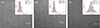 |
Fig. 1 SEM micrographs showing the morphology after the Al layer deposition process: (a) 2 nm, (b) 4 nm, and (c) 6 nm. |
The enhancement factor varies depending on the shape and distance of the metallic nanoaggregates [32]. Taking this into account, we collected the fluorescence emission across the entire surface of the nanostructured platform. Due to the resulting surface filling factor and the consistent shapes and sizes of the nanoaggregates achieved under the same deposition or annealing conditions, the MEF remains relatively unchanged when analysing new samples, ensuring high reproducibility. The steady-state fluorescent emission spectra of CV, NR, and RB on nanostructured Al films were compared to a reference consisting of a silicon substrate without metasurfaces coated with fluorophore. Figure 2 shows the obtained fluorescence spectra, with an inset graph on a logarithmic scale illustrating the magnitude orders of the best enhancement result. The fluorescence enhancement depends on spectral overlap between excitation/emission bands and plasmonic scattering/near-field response. For all three fluorophores, nanostructured Al induced changes in fluorescence intensity without significantly affecting the characteristic spectral band profiles. This indicates that the dominant interaction is photonic (near-field/plasmonic) and not a chemical modification of the fluorophore. Such behaviour is largely associated with MEF, in which local electromagnetic fields and modified radiative decay rates can increase emission intensity without necessarily changing spectral maxima.
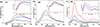 |
Fig. 2 Fluorescence intensity spectra of a) CV, b) NR and c) RB on nanostructured Al films; dashed black: reference, green/blue/red: 2/4/6 nm Al. Inset are the MEF with logarithmic y scale. |
The EF are calculated relative to the respective emission maxima of each fluorophore. The values vary depending on the type of fluorophore – specifically, their quantum efficiency – rather than the layer thickness. For NR, we obtain a maximum EF of approximately 3.2 when we use a thin film of 4 nm thickness. In the meantime, for CV and RB, we obtain maximum EF values of 2.8 and 7.7, respectively, when we use a thickness of 6 nm.
Silver thin films with thicknesses of 15 nm, 20 nm, and 25 nm were deposited on silicon and subsequently subjected to thermal annealing. This treatment induced the formation of metal aggregates, resulting in randomly distributed meta-atom structures. Figure 3 shows SEM images of the annealed Ag layers at all three thicknesses, revealing the morphology of the formed nanostructures. SEM analysis demonstrates a systematic thickness-dependent morphological transition in the annealed Ag films. The 15 nm film exhibits isolated, quasi-ellipsoidal nanoparticles with minimal inter-particle connectivity. At 20 nm, partial aggregation occurs, forming bigger anisotropic islands with increased contact between adjacent structures. The 25 nm film displays complete percolation, characterized by an interconnected spiderweb-like metallic network.
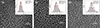 |
Fig. 3 SEM micrographs showing the morphology obtained following the deposition of Ag layers structured by annealing: (a) 15 nm, (b) 20 nm, (c) 25 nm. |
Similar to Al films, the particle size statistics for Ag nanoaggregates (see inset in Fig. 3) show an increase in mean particle size with layer thickness: 124 nm for the 15 nm layer, 189 nm for the 20 nm layer, and 234 nm for the 25 nm layer. The corresponding standard deviation increases as well, from 34 nm to 57 nm. Furthermore, the surface filling factor, which is defined as the fraction of the substrate surface covered by Ag nanoparticles, increases with layer thickness. Specifically, it increases from 32% for the 15 nm layer, to 37% for the 20 nm layer, and to 76% for the 25 nm layer. This increase in surface coverage reflects the transition from isolated nanoparticle regimes toward a densely packed morphology, which is consistent with enhanced surface diffusion, particle aggregation, and lateral growth during thermal treatment.
Figure 4 presents the fluorescence emission spectra of CV, NR, and RB fluorophores films deposited on thermally annealed Ag nanostructures, in comparison with a reference substrate, with an inset graph on a logarithmic scale. The fluorescence measurements reveal substantial intensity increases relative to the reference for all fluorophores, with EF dependent on Ag thickness and fluorophore: for CV the EF increases from ≈6.8 (15 nm) to ≈10 (20 nm) and ≈19 (25 nm), for NR from ≈2.4 (15 nm) to ≈4 (20 nm) and ≈4.4 (25 nm), and for RB from ≈2 (15 nm) to ≈4 (20 nm) and ≈6 (25 nm).
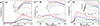 |
Fig. 4 Fluorescence intensity spectra of a) CV, b) NR and c) RB on nanostructured Ag films; dashed black: reference, green/blue/red: 15/20/25 nm Ag. Inset are the MEF with logarithmic y scale. |
Table 2 summarizes the fluorescence EF for CV, NR, and RB deposited on nanostructured Al and Ag films of varying thicknesses. For Al substrates, moderate enhancement is observed, with EF values increasing with thickness for CV and RB and showing an optimum at 4 nm for NR. In contrast, Ag films exhibit substantially stronger enhancement for all fluorophores, particularly at larger Ag thicknesses. CV shows the highest enhancement overall, reaching EF = 19 on the 25 nm Ag film, while RB and NR reach maxima of EF = 6 and EF = 4.4, respectively. These results indicate that Ag nanostructures support more efficient plasmon-mediated fluorescence enhancement than Al under the studied conditions, with the degree of enhancement strongly dependent on both the fluorophore and metal layer thickness. Furthermore, the highest EF are obtained when using the 25 nm Ag film. The high filling factor observed for this metasurface platform suggests the onset of particle percolation, which influences significantly the plasmonic coupling. Additionally, the spiderweb pattern that forms after annealing – consisting of a high number of sharp angles – significantly intensifies the localized electromagnetic field.
Fluorescence enhancement factors for CV, NR, RB on nanostructured Al films (2, 4, 6 nm) and Ag films (15, 20, 25 nm).
4. Conclusion
In this study we presented a simple plasmonic metasurface approach for enhancing fluorescence of low quantum yield dyes using thin film derived nanostructures. We performed thermal annealing on Ag films (15–25 nm), and deposited mass equivalent ultrathin Al films (2–6 nm) to develop large plasmonic metasurface platforms comprising of randomly configurate metallic nano-aggregates. The native oxide of studied metals provides the separation required to partially mitigate the extreme near-field quenching while enabling coupling to localized plasmonic fields from nanoscale features. We investigated the behaviour of the fluorescence intensity for Crystal Violet, Nile Red, and Rose Bengal in the presence of metal nanostructures. The EF are calculated relative to the respective emission maxima of each fluorophore. The values vary depending on the type of fluorophore – specifically, their quantum efficiency – rather than the layer thickness. For Al, promising results concerning fluorescence intensity enhancement were obtained using 6 nm mass equivalent layers, with the best EF for Rose Bengal. At low thicknesses (e.g., 6 nm), Al forms monodisperse, nearly periodic nanostructures with very low heights. This leads to a uniform distribution of localized field enhancements. Since the structures are uniformly spaced, a large portion of the fluorophores can interact with the plasmonic resonances, resulting in consistent enhancement.
For Ag the fluorescence measurements revealed substantial intensity increases, with EF dependent on Ag thickness and fluorophore, the best result was obtained for Crystal Violet for 25 nm with an EF of 19. Silver forms large aggregates, evolving from hemispherical shapes to percolated spiderweb at a thickness of 25 nm. The enhancement occurs via two mechanisms: i) height matching ensures most molecules are within the plasmonic interaction zone of the 25 nm structures, and ii) natural spacing, where the native oxide layer prevents quenching by maintaining distance between the dyes and metal surface. Although aluminium is suitable for thin layers, the taller percolated structures offered by annealed silver thicker films exhibit significant enhancement of fluorescence emission.
The proposed low-cost, lithography-free platforms offer a versatile approach for enhancing the broadband spectral emission of a variety of fluorophores without specifically tailoring the geometry for each chromophore, providing a scalable, morphology-driven, plasmon-enhanced fluorescence. Furthermore, the fabrication method used in this study allows for nanostructuring large wafers of various substrate – silicon, glass, or ceramics, for a multitude of hands-on applications requiring a rapid response (e.g. refractive index-based sensors, fluorescence sensors, photocatalysis, etc.).
Funding
This research was funded by the Core Program of IMT-Bucharest within the National Research Development and Innovation Plan 2022-2026, carried out with the support of Romanian Ministry of Research, Innovation and Digitization, project no. 2307.
Conflicts of interest
The authors have nothing to disclose.
Data availability statement
This article has no associated data generated and/or analyzed.
Author contribution statement
Conceptualization, R.T. and V.A.; Methodology, D.C.; Validation, V.A, C.K. and R.T; Formal Analysis, V.A. and R.T.; Investigation, V.A., I.M., O.B., A.D.; Data Curation, V.A., O.B., and I.M.; Writing – Original Draft Preparation, V.A. and R.T.; Writing – Review & Editing, V.A., R.T., D.C. and C.K.; Supervision, R.T., D.C. and C.K.; Project Administration, R.T. and D.C.; Funding Acquisition, R.T. and D.C.
Acknowledgments
The authors acknowledge Gabriel Craciun for electron beam deposition using Elettrorava system.
References
- Huang Y, Zhai J, Liu L, Shang Z, Zhang X, Huang H, Shen B, Chen G, Recent developments on nanomaterial probes for detection of pesticide residues: a review, Anal Chim Acta. 1215, 339974 (2022). https://doi.org/10.1016/j.aca.2022.339974. [Google Scholar]
- Bai L et al., Molecular imprinted polymer capped luminescent metal-organic framework for the determination of pyrethroids and its metabolite, Microchem J. 193, 109047 (2023). https://doi.org/10.1016/j.microc.2023.109047. [Google Scholar]
- Narasimhan V, Siddique RH, Hoffmann M, Kumar S, Choo H, Enhanced broadband fluorescence detection of nucleic acids using multipolar gap-plasmons on biomimetic Au metasurfaces, Nanoscale 11, 3750 (2019). https://doi.org/10.1039/C9NR03178B. [Google Scholar]
- Xu J, Morton W, Jones D, Tabish TA, Ryan MP, Xie F, Significant quantum yield enhancement for near infrared fluorescence dyes by silica templated silver nanorods, Appl. Phys. Rev. 9, 031406 (2022). https://doi.org/10.1063/5.0082187. [Google Scholar]
- Traverso AJ et al., Low-loss, centimeter-scale plasmonic metasurface for ultrafast optoelectronics, Optica 8(2), 202 (2021). https://doi.org/10.1364/OPTICA.400731. [Google Scholar]
- Bardhan R, Grady NK, Cole JR, Joshi A, Halas NJ, Fluorescence enhancement by Au nanostructures: nanoshells and nanorods, ACS Nano. 3(3), 744 (2009). https://doi.org/10.1021/nn900001q. [Google Scholar]
- Yu L, Yang Y, Jiang X, Li Y, He X, Chen L, et al. A self-calibrating ratiometric fluorescence sensor with photonic crystal-based signal amplification for the detection of tetracycline in food, Food Chem. 451, 139418 (2024). https://doi.org/10.1016/j.foodchem.2024.139418. [Google Scholar]
- He H, Muhammad P, Guo Z, Peng Q, Lu H, Liu Z, Controllably prepared molecularly imprinted core-shell plasmonic nanostructure for plasmon-enhanced fluorescence assay, Biosens. Bioelectron. 146, 111733 (2019). https://doi.org/10.1016/j.bios.2019.111733. [Google Scholar]
- Lin J-S, Radjenovic PM, Jin H, Li J-F, Plasmonic core–shell nanoparticle enhanced spectroscopies for surface analysis, ACS Publ. 93(17), 6573 (2021). https://doi.org/10.1021/acs.analchem.1c00233. [Google Scholar]
- Xu J et al., Shell-isolated nanoparticle-enhanced Raman and fluorescence spectroscopies: synthesis and applications, Adv. Optic. Mater. 6(4), 1701069 (2018). https://doi.org/10.1002/adom.201701069. [Google Scholar]
- Iwanaga M, Productive biosensing techniques empowered by all-dielectric metasurfaces, Front. Bioeng. Biotechnol. 12. (2025). https://doi.org/10.3389/fbioe.2024.1484638. [Google Scholar]
- Khan SA et al., Optical sensing by metamaterials and metasurfaces: from physics to biomolecule detection, Adv. Opt. Mater. 10(18), 2200500 (2022). https://doi.org/10.1002/adom.202200500. [Google Scholar]
- Montaño-Priede JL et al., An overview on plasmon-enhanced photoluminescence via metallic nanoantennas, Nanophotonics 13(26), 4771–4794 (2024). https://doi.org/10.1515/nanoph-2024-0463. [Google Scholar]
- Gartia MR, Hsiao A, Sivaguru M, Chen YC, Liu GL, Enhanced 3D fluorescence live cell imaging on nanoplasmonic substrate, Nanotechnology 22(36), 365203–365203 (2011). https://doi.org/10.1088/0957-4484/22/36/365203. [Google Scholar]
- Hohenberger E, Freitag N, Rosenmann D, Korampally V, A facile route towards large area self-assembled nanoscale silver film morphologies and their applications towards metal enhanced fluorescence, Sens. Actuators B Chem. 249, 549–557 (2017). https://doi.org/10.1016/J.SNB.2017.04.012. [Google Scholar]
- Lu H, et al., Broadband near-field enhancement in the macro-periodic and micro-random structure with a hybridized excitation of propagating Bloch-plasmonic and localized surface-plasmonic modes, Nanoscale 7(40), 16798–16804 (2015). https://doi.org/10.1039/C5NR03391H. [Google Scholar]
- González-Alcalde AK, Rojas-Martinez IY, Reyes-Coronado A, Broadband antireflective random metasurfaces, J. Opt. Soc. Am. B 38(6), 1974–1983 (2021). https://doi.org/10.1364/JOSAB.420085. [Google Scholar]
- Anăstăsoaie V et al., Influence of Random Plasmonic Metasurfaces on Fluorescence Enhancement, Materials 15(4), 1429 (2022). https://doi.org/10.3390/ma15041429. [Google Scholar]
- Tasolamprou AC, et al., Highly ordered laser imprinted plasmonic metasurfaces for polarization sensitive perfect absorption, Sci. Rep. 12(1), 19769 (2022). https://doi.org/10.1038/s41598-022-21647-w. [Google Scholar]
- Skoulas E et al., Laser induced periodic surface structures as polarizing optical elements, Appl. Surf. Sci. 541, 148470 (2020). https://doi.org/10.1016/j.apsusc.2020.148470. [Google Scholar]
- Khatua S, Paulo PMR, Yuan H, Gupta A, Zijlstra P, Orrit M, resonant plasmonic enhancement of single-molecule fluorescence by individual gold nanorods, ACS Nano. 8(5), 4440 (2014). https://doi.org/10.1021/nn406434y. [Google Scholar]
- Xu J et al., Significant quantum yield enhancement for near infrared fluorescence dyes by silica templated silver nanorods, Appl. Phys. Rev. 9(3), 031406 (2022). https://doi.org/10.1063/5.0082187. [Google Scholar]
- Brey LA, Schuster GB, Drickamer HG, High pressure studies of the effect of viscosity on fluorescence efficiency in crystal violet and auramine, O. J. Chem. Phys. 67, 2648 (1977). https://doi.org/10.1063/1.435177. [Google Scholar]
- Sackett DL, Wolff J, Nile red as a polarity-sensitive fluorescent probe of hydrophobic protein surfaces, Anal. Biochem. 167(2), 228 (1987). https://doi.org/10.1016/0003-2697(87)90157-6. [Google Scholar]
- Quest Database™ Quantum Yield [Rose Bengal] (AAT Bioquest, Inc., 25 Jan. 2026), https://www.aatbio.com/resources/quantum-yield/rose_bengal. [Google Scholar]
- Jones RR et al., Dense arrays of nanohelices: Raman scattering from achiral molecules reveals the near-field enhancements at chiral metasurfaces, Adv. Mater. 35(34), 2209282 (2023). https://doi.org/10.1002/adma.202209282. [Google Scholar]
- Synak A et al., Enhanced emission of Nile Red on plasmonic platforms, Optical Mater. 78, 82 (2018). https://doi.org/10.1016/j.optmat.2018.02.009. [Google Scholar]
- Swayam P et al., Microscopic perspective of synergy between localized surface plasmon resonance and disruption of dye aggregates in metal nanoparticle-enhanced fluorescence, ACS Appl. Nano Mater. 6(19), 17539 (2023). https://doi.org/10.1021/acsanm.3c02734. [Google Scholar]
- Gabudean AM, Focsan M, Astilean S, Gold nanorods performing as dual-modal nanoprobes via metal-enhanced fluorescence (MEF) and surface-enhanced Raman scattering (SERS), J. Phys. Chem. C 116(22), 12240 (2012). https://doi.org/10.1021/jp211954m. [Google Scholar]
- Hsing-Hui L, Chen I-C, Study of the interaction between gold nanoparticles and rose bengal fluorophores with silica spacers by time-resolved fluorescence spectroscopy, J. Phys. Chem. C 119(47), 26663 (2015). https://doi.org/10.1021/acs.jpcc.5b08477. [Google Scholar]
- Knight MW et al., Aluminum for plasmonics, ACS Nano. 8(1), 834 (2014). https://doi.org/10.1021/nn405495q. [Google Scholar]
- Zhao X, Alizadeh MH, Reinhard BM, Harnessing leaky modes for fluorescence enhancement in gold-tipped silicon nanowires, J. Phys. Chem. C. 120, 37 (2016). https://doi.org/10.1021/acs.jpcc.5b11702. [Google Scholar]
All Tables
Fluorescence enhancement factors for CV, NR, RB on nanostructured Al films (2, 4, 6 nm) and Ag films (15, 20, 25 nm).
All Figures
|
Fig. 1 SEM micrographs showing the morphology after the Al layer deposition process: (a) 2 nm, (b) 4 nm, and (c) 6 nm. |
| In the text | |
|
Fig. 2 Fluorescence intensity spectra of a) CV, b) NR and c) RB on nanostructured Al films; dashed black: reference, green/blue/red: 2/4/6 nm Al. Inset are the MEF with logarithmic y scale. |
| In the text | |
|
Fig. 3 SEM micrographs showing the morphology obtained following the deposition of Ag layers structured by annealing: (a) 15 nm, (b) 20 nm, (c) 25 nm. |
| In the text | |
|
Fig. 4 Fluorescence intensity spectra of a) CV, b) NR and c) RB on nanostructured Ag films; dashed black: reference, green/blue/red: 15/20/25 nm Ag. Inset are the MEF with logarithmic y scale. |
| In the text | |
Current usage metrics show cumulative count of Article Views (full-text article views including HTML views, PDF and ePub downloads, according to the available data) and Abstracts Views on Vision4Press platform.
Data correspond to usage on the plateform after 2015. The current usage metrics is available 48-96 hours after online publication and is updated daily on week days.
Initial download of the metrics may take a while.