


Fig. 1
Download original image
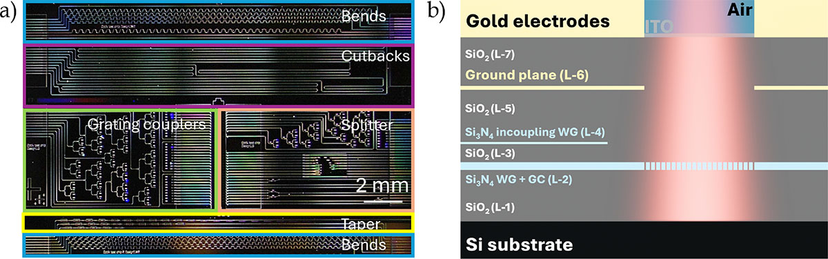
a) Optical micrograph of the fabricated Si3N4 PIC, showing different functional regions: WG cutback structures (purple), bend and bend-shift loss structures (cyan), EBL–OL taper structures (yellow), grating coupler (green) and splitter test structures (orange). b) Targeted multilayer stack. From bottom to top: Si substrate, SiO2 BOX (L-1), Si3N4 WG-GC (L-2) and WG for light incoupling layers (L-4) separated by a 1.25 μm thick SiO2 buffer layer (L-3). Above these, an additional SiO2 buffer layer is followed by a gold ground plane, 3 μm thick SiO2 spacer, and a top gold layer used as the electrodes. Holes in the electrodes are covered with an ITO layer. The red cone illustrates the beam emitted by the GC.
Current usage metrics show cumulative count of Article Views (full-text article views including HTML views, PDF and ePub downloads, according to the available data) and Abstracts Views on Vision4Press platform.
Data correspond to usage on the plateform after 2015. The current usage metrics is available 48-96 hours after online publication and is updated daily on week days.
Initial download of the metrics may take a while.