| Issue |
J. Eur. Opt. Society-Rapid Publ.
Volume 21, Number 2, 2025
|
|
|---|---|---|
| Article Number | 34 | |
| Number of page(s) | 6 | |
| DOI | https://doi.org/10.1051/jeos/2025030 | |
| Published online | 16 July 2025 | |
Research Article
High-efficiency broadband grating out-coupler for thick silicon waveguides with a tuned SiGe layer
1
Center for Photonics Sciences, University of Eastern Finland, Yliopistokatu 7, PO Box 111, 80101, Joensuu, Finland
2
VTT Technical Research Center of Finland, Tietotie 3, 02150 Espoo, Finland
3
Xanadu Quantum Technologies, 24th fl, 777 Bay Street, Toronto, ON M5B 2H7, Canada
* Corresponding author: This email address is being protected from spambots. You need JavaScript enabled to view it.
Received:
25
April
2025
Accepted:
12
June
2025
Abstract
We design a novel grating out-coupler while maintaining a Gaussian-shaped far-field output. The approach is based on the patterning of a grating in a SiGe layer on the top surface of a 3-μm-thick Si waveguide. The grating aims at coupling the guided signal into a beam vertically out from the surface of the chip, i.e., out-coupling. The use of a high refractive index alloy, i.e., silicon-germanium, allows a tunability of the effective index of the guided mode and to modify the field distribution enabling a higher efficiency of the grating. It yields a theoretical efficiency of 75% at the central wavelength of 1583 nm. The overall length of this grating coupler is 500 μm, and the output light is detected at 1 μm above the grating. This type of long grating coupler is intended to be eventually used as sensor in LiDAR (Light detection and ranging) applications.
Key words: Silicon germanium / Grating out-coupler / Long device / Broad-band / LiDAR applications
The affiliation of this author has changed during the publication process. He was affiliated to VTT Technical Research Center of Finland while working on this paper.
© The Author(s), published by EDP Sciences, 2025
 This is an Open Access article distributed under the terms of the Creative Commons Attribution License (https://creativecommons.org/licenses/by/4.0), which permits unrestricted use, distribution, and reproduction in any medium, provided the original work is properly cited.
1 Introduction
Silicon photonics has been in the spotlight for many years owing to the revolution it has undergone. This platform enabled to perform, on-a-chip, nonlinear optics [1], high speed optical communications [2], mid-infrared devices [3], photonics crystals [4], optoelectronic integrated circuits [5], and more recently, LiDAR (light detection and ranging) sensors [6]. Silicon-on-insulator platforms are proven to play a significant role in next-generation optical interconnects as it already shows [7–9]. Beam steering mechanism constitutes an important part of LiDAR systems. In our previous publication [10], optical phased arrays have been demonstrated successfully to carry out non-mechanical one-dimensional (1D) beam steering. However, two-dimensional (2D) beam steering and, ultimately, angle scanning, demand extensive device geometry development and more advanced steering mechanisms.
Despite the numerous high-performance optical components available on silicon-on-insulator (SOI) platform, in and out light coupling to and from silicon chips remain a challenge. The issue of the large modal mismatch between the waveguide and single-mode fibre, mostly due to the refractive index difference, is met with mainly two solutions, i.e., edge coupling and vertical grating couplers [11–13].
Considering a common edge out-coupling in silicon waveguide, the output beam signal remains relatively well collimated in the horizontal direction, but it tends to quickly diverge vertically, because the waveguide is thin. It yields additional optical component, e.g., lensed, to collimate the output beam, which is one requirement in LiDARs. An alternative approach is to use a grating out-coupler, i.e., patterning a grating on the surface of the waveguide. It allows the beam to propagate out of the waveguide, eventually perpendicularly to the surface of the chip. Such a vertical grating out-coupler offers a flexibility in terms of measurement techniques and require less post-processing as compared to the edge couplers [14], which is an advantage for the development of portable devices. Researchers have been working on the grating on micron-scale waveguides for single-mode fibre coupling [15] and have demonstrated experimentally a grating coupler in 1.5 μm thick SOI rib waveguides with a 3 dB bandwidth. Apart from the fundamental mode, higher number of modes can also couple to these thicker waveguides. A diffraction grating operating in reflection has also been investigated [3] to allow beam steering in the vertical direction by tuning the wavelength of the light source.
In addition to the aforementioned difficulties, the size of the beam is one of the biggest challenges for LiDAR applications. Creating a large beam (>100 μm size) is more demanding than simply coupling to a few-micrometer single mode fiber, because a part of the signal intensity is already lost during the propagation along the grating [11, 16]. To obtain a large beam with a controlled intensity cross-section over the surface of the grating out-coupler, it is necessary to increase the strength of the grating gradually along the propagation direction.
This paper is devoted to the theoretical study of an out-coupler grating on thick silicon platform for LiDAR applications. The aim is to create a large Gaussian-shaped beam (around 500 μm) propagating in a vertical direction with respect to the plane of the chip. Although the work is purely based on theoretical considerations and simulations, tolerances, and fabrication constraints as well as material dispersion properties are constantly considered.
2 Design
The overall design is presented in Figure 1a. The hypothesis considered at start is a 3 μm thick and 2 μm wide silicon strip waveguide supporting quasi-TE (electric field along y-axis) fundamental mode, as well as many other modes. Light is coupled adiabatically from a single-mode (SM) rib waveguide into the strip waveguide, so that only this fundamental TE mode is excited, and the waveguide effectively acts as a SM waveguide [17]. The modal intensity distribution is given in Figure 1b. The high confinement of the mode inside the large high-refractive index waveguide makes the design of grating out-coupler directly on top of it nearly impossible for high efficiency. The mode needs to be pushed closer to the surface. We propose the inclusion of a top layer of higher refractive index material, namely, SiGe. The fundamental mode establishes in this layer, on which a binary grating can be patterned to extract the field. The modal distribution is presented in Figure 1c.
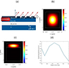 |
Fig. 1 (a) Diagram of the designed grating out-coupler. (b, c) Intensity distribution of the fundamental quasi-TE mode showing the confinement in (b) a 2 × 3 μm2 Si waveguide (thick SOI platform) waveguide and (c) in a 911 nm thick SiGe layer deposited on top the same Si waveguide. (d) transmission as a function of the thickness of the SiGe layer. |
The refractive index of SiGe depends on the ratio between Si and Ge. In the C-band, germanium absorbs light, and it is important to find a trade-off between the amount of Ge which increases the refractive index of the top layer and the overall absorption of this layer. The refractive index of this layer affects the efficiency of the grating that will be patterned on it as well as the necessary thickness.
SiGe epitaxial growth procedure is a silicon complementary metal-oxide-semiconductor (CMOS) compatible fabrication technologies bringing significant benefits to SiGe-based devices [18]. We chose a stoichiometry corresponding to 80% of Si and 20% of Ge. It yields a refractive index n SiGe = 3.606 at λ = 1550 nm. According to the transmission through an SiGe layer measured for several thicknesses, we opt for a thickness t SiGe = 911 nm. Deviations from this thickness result in multiple peaks in the far-field distribution. This behavior can be attributed to phase mismatch and interference effects. Additionally, non-optimal thicknesses lead to excitation of higher-order diffraction modes. These results highlight the critical role of SiGe thickness in achieving efficient coupling and directional emission. Simulations performed using ANSYS Lumerical determined the effective index of the guided mode (for the structure with an SiGe layer) n eff = 3.59 at λ = 1550 nm. One can now focus on the design of the grating enabling the outcoupling of light. We aim at a broadband extraction of the field and a maintained Gaussian shape of the output beam.
Let us start with a simple binary grating etched in the SiGe. The working principle of outcoupling with a grating is based on the phase matching condition or the Bragg condition which describes the relation between the propagation constant β of the fundamental guided mode and the modulus of the output wavevector of the desired diffraction order from the grating, k
o, as shown in equation (1) [11]. (1)where G = 2π/Λ is the grating vector for a structure of period Λ and m is the diffraction order of the grating. Based on the Bragg condition, we can predict which grating order should propagate. The angle of the output beam (θ) depends on the parameters of the grating such as period, etching depth (h) and fill factor (f). The output angle can be tailored according to the geometrical properties of the structure. The fill factor, defined as the ratio of the etched area to the total grating period, determines the weighting between the refractive indices of the etched and non-etched portion. Consequently, effective index (N
eff) can be stated as in equation (2).
(1)where G = 2π/Λ is the grating vector for a structure of period Λ and m is the diffraction order of the grating. Based on the Bragg condition, we can predict which grating order should propagate. The angle of the output beam (θ) depends on the parameters of the grating such as period, etching depth (h) and fill factor (f). The output angle can be tailored according to the geometrical properties of the structure. The fill factor, defined as the ratio of the etched area to the total grating period, determines the weighting between the refractive indices of the etched and non-etched portion. Consequently, effective index (N
eff) can be stated as in equation (2). (2)where n
o is effective index of the non-etched portion and n
e is the effective index of the etched portion of the grating. Fill factor has been plotted against the effective index and we can see the trend in the Figure 2a, where N
eff increases with the increase in the fill factor.
(2)where n
o is effective index of the non-etched portion and n
e is the effective index of the etched portion of the grating. Fill factor has been plotted against the effective index and we can see the trend in the Figure 2a, where N
eff increases with the increase in the fill factor.
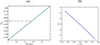 |
Fig. 2 (a) Theoretical fill factor plot against n eff. (b) Theoretical correspondence between the diffracted angle and the central wavelength. |
The period of the grating is kept constant throughout the structure. This period can be calculated using the Bragg condition as equation (3). (3)
(3)
where n bg is the refractive index of the cladding layer and n eff is the effective index of the guided mode with respect to the etch depth of the grating. λ c is the central operating wavelength of the optical beam interacting with the grating. Theoretical correspondence between the central wavelength and diffracted angle is represented in Figure 2b.
To perform a beam shaping of the output light, the strength of the grating is changed, and therefore, the intensity distribution varied, along the propagation direction through a controlled modification of the fill factor. By carefully adjusting the out-coupling efficiency as a function of the signal intensity in the channel waveguide and the geometrical position of the grating, the shape of the output beam can be maintained Gaussian. This is achieved by varying the fill factor to obtain progressively a stronger out-coupling. The fill factor of the ending part of the grating is again tuned to a corresponding very weak efficiency.
The grating out coupler being intended to be broadband, the dispersion of SiGe is considered in the calculations. The dielectric dispersion shows a slight decrease of the refractive index from 3.604 to 3.612 along the wavelength range of interest 1530 nm–1580 nm [19]. It is to be noted that the refractive index and dispersion of SiGe depends on the percentage composition of the material. A careful ratio must be chosen in order to obtain a material with low absorption (low in Ge) but high refractive index (high in Ge). For the purpose of this current study we chose 80% of Si for 20% of Ge.
An efficiency curve of the grating has been obtained through simulations in which the fill factor is varied. The highest efficiency of outcoupling was obtained by maintaining the height of silicon germanium constant at 911 nm and a partial etch depth of the SiGe layer of 195 nm. It yields an equation, extracted from the calculated efficiencies η along the propagation direction z, given in equation (4) as a function of the fill factor of the grating. (4)
(4)
where η(ff) is the efficiency and the variable ff corresponds to the fill factor in the different regions of the grating. a, b, and c are constants determining the parameters of the Gaussian beam shape.
3 Simulation results
2D-FDTD (finite-difference Time-domain) simulations are performed using ANSYS Lumerical commercial software. The frequency domain power transmission is obtained from the monitor placed at the topside of the grating and is calculated through the following formula: (5)
(5)
where T(ω) is the normalized transmission as a function of frequency, P(ω) is the pointing vector and dS is the surface normal.
All parameters of the grating, i.e., the height of the grating layer, etching depth, and period, have been varied and studied to optimize the efficiency of the grating. The period set the central wavelength of highest efficiency for each section N of the complete grating, see Figure 3a for Λ = 370 nm, 380 nm, 390 nm, 400 nm corresponding to λ c = 1555 nm, 1565 nm, 1570 nm, and 1585 nm, respectively.
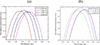 |
Fig. 3 (a) Central wavelength variation with the grating period. (b) Transmission curves at varying etching depth. |
Considering Λ = 370 nm corresponding to a maximal efficiency at λ c = 1555.5 nm, the etching depth h and the height of the grating, i.e., SiGe layer thickness t, are investigated to optimize further the transmission above the grating. Transmission curves examples are shown in Figure 3b for three etching depths. h influences the central wavelength and the efficiency. The optimum is found for h = 195 nm. Once the geometry is determined for each grating section, a final FDTD simulation of the entire grating is performed. The height of the SiGe layer is set to t = 911 nm and the etching depth is h = 195 nm. The period is set to Λ = 370 nm.
The field distribution in a plane along the propagation direction (xz-plane) is given in Figure 4a. Even though the Bragg condition allows the outcoupling at an angle of 0°, usually a tilt angle is preferred. This is explained by the presence of strong back reflections due to second order diffraction [20]. The simulated angle of the output beam at the central wavelength, i.e., 1555 nm, is 34° which is close to the calculated angle, i.e., 37° through the Bragg condition in equation (3).
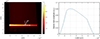 |
Fig. 4 (a) Electric field distribution in a plane parallel to the propagation direction. (b) Electric field amplitude at 1555 nm. |
The efficiency along the topside of the grating can then be calculated from equation (6) using data extracted from the FDTD simulations. Intensity is collected and sum over a line located at 1 μm above the grating. The sum corresponds then to the far field intensity.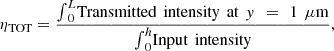 (6)
(6)
where L is the total length of the grating and h the height of the SiGe guiding layer. The out-coupling efficiency through this long grating is 75%. The electric field amplitude at 12 μm from the grating surface can be seen from Figure 4b.
The design considers the targeted broadband operation of the device. A variation in wavelength implies a variation in the output angle and in efficiency. Figure 5a shows the far-field intensity as a function of the wavelength and its angle dependence.
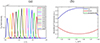 |
Fig. 5 (a) Far-field Intensity in terms of angle and wavelength. (b) Transmittance curves at different directions of the structure. |
The transmission as a function of the wavelength along three characteristic locations of the structure, i.e., above the grating, under the grating, at the waveguide output, can be observed in Figure 5b.
4 Conclusion
We have presented the design and expected properties of a novel vertical grating coupler on thick SOI platform and operating in the telecom C-band. Such a structure is enabled by the use of high refractive index material, i.e., SiGe, deposited on the top side of the waveguide at the selected places for out-coupling. The SiGe layer pulls the mode upwards for an increased overlap of light with grating leading to a better control of the out-coupling efficiency and therefore a control shape of the output beam. The length of the grating is 500 μm and the extraction efficiency is 75% at the top side of the grating. Such a grating is intended to be performed on the output waveguides of integrated LiDAR for two-dimensional beam steering.
Funding
We would like to acknowledge Research Council of Finland Flagship for Photonics Research and Innovation (PREIN) for funding this based on the μLiDAR applications (funding decisions 346518 and 346545).
Conflicts of interest
The authors declare no conflicts of interest.
Data availability statement
Data underlying the results presented in this paper are not publicly available at this time but may be obtained from the authors upon reasonable request.
Author contribution statement
Conceptualization, Matteo, Timo; Design, Sidra, Matteo, Matthieu; Software and simulations, Sidra, Isaac; Analysis, Sidra; Writing, Original Draft Preparation, Sidra; Writing, Review & Editing, Timo and Matthieu; Supervision, Matteo, Timo, and Matthieu.
References
- Leuthold J, Koos C, Freude W, Nonlinear silicon photonics, Nat. Photonics 4, 535 (2010). https://doi.org/10.1038/nphoton.2010.185. [Google Scholar]
- Zhou X, Yi D, Chan DWU, Tsang HK, Silicon photonics for high-speed communications and photonic signal processing, npj Nanophotonics 1, 27 (2024). https://doi.org/10.1038/s44310-024-00024-7. [Google Scholar]
- Baehr-Jones T, et al., Silicon-on-sapphire integrated waveguides for the mid-infrared, Opt. Express 18, 12127 (2010). https://doi.org/10.1364/OE.18.012127. [Google Scholar]
- Geppert T, Schilling J, Wehrspohn R, Gösele U, Silicon-based photonic crystals, Topics Appl. Phys. 94, 295 (2004). https://doi.org/10.1007/978-3-540-39913-1_9. [Google Scholar]
- Leheny RF, Optoelectronic integrated circuits, in International Technical Digest on Electron Devices, (IEEE, 1990), p.7. https://doi.org/10.1109/IEDM.1990.237238. [Google Scholar]
- Xu C, Liu C, Ding Y, Wang R, Wu A, FMCW LiDAR with a coherent receiver chip based on 3 μm SOI photonics platform, Results Phys. 57, 107327 (2024). https://doi.org/10.1016/j.rinp.2024.107327. [Google Scholar]
- Reed G, in Optical interconnects. Springer Series in Optical Sciences, vol. 119, edited by L. Pavesi, G. Gerard (Springer, Berlin, Heidelberg, 2007), p. 161–203. https://doi.org/10.1007/978-3-540-28912-8_7. [Google Scholar]
- Rahim A, Spuesens T, Baets R, Bogaerts W, Open-access silicon photonics: current status and emerging initiatives, Proc. IEEE 106, 2313 (2018). https://doi.org/10.1109/JPROC.2018.2878686. [Google Scholar]
- Thomson D, et al., Roadmap on silicon photonics, J. Opt. 18, 073003 (2016). https://doi.org/10.1088/2040-8978/18/7/073003. [Google Scholar]
- Muntaha ST, et al., 3D printed lenses for vertical beam collimation of optical phased arrays, 3D Print. Addit. Manuf. 11, e1227 (2024). https://doi.org/10.1089/3dp.2022.0314. [Google Scholar]
- Marchetti R, Lacava C, Carroll L, Gradkowski K, Minzioni P, Coupling strategies for silicon photonics integrated chips, Photon. Res. 7, 201 (2019). https://doi.org/10.1364/PRJ.7.000201. [Google Scholar]
- Mu X, Wu S, Cheng L, Fu H-Y, Edge couplers in silicon photonic integrated circuits: a review, Appl. Sci. 10, 1538 (2020). https://doi.org/10.3390/app10041538. [Google Scholar]
- Wang Y, Yun H, Jaeger NAF, Chrostowski L, Broadband bidirectional vertical grating coupler, in 2016 Optical Fiber Communications Conference and Exhibition (OFC), Anaheim, CA, USA, March 20–24 (IEEE, 2016), p. 1. [Google Scholar]
- Wang Y, Grating coupler design based on silicon-on-insulator [Online] (2013). Available at https://open.library.ubc.ca/collections/24/items/1.0073806. [Google Scholar]
- Alonso-Ramos C, et al., Single-etch grating coupler for micrometric silicon rib waveguides, Opt. Lett. 36, 2647 (2011). https://doi.org/10.1364/OL.36.002647. [Google Scholar]
- Nambiar S, Sethi P, Selvaraja SK, Grating-assisted fiber to chip coupling for SOI photonic circuits, Appl. Sci. 8, 1142 (2018). https://doi.org/10.3390/app8071142. [Google Scholar]
- Aalto T, et al., Open-Access 3-μm SOI waveguide platform for dense photonic integrated circuits, IEEE J. Sel. Topics Quantum Electron. 25, 1 (2019). [Google Scholar]
- Sood AK, et al., in Advances in Optical Fiber Technology, edited by Moh Yasin, H. Arof, S.W. Harun (IntechOpen, Rijeka, 2015). https://doi.org/10.5772/59065. [Google Scholar]
- Jellison GE, Haynes TE, Burke HH, Optical functions of silicon-germanium alloys determined using spectroscopic ellipsometry, Opt. Mater. 2, 105 (1993). https://doi.org/10.1016/0925-3467(93)90035-Y. [Google Scholar]
- Cheng L, Mao S, Li Z, Han Y, Fu HY, Grating couplers on silicon photonics: design principles, emerging trends and practical issues, Micromachines 11, 666 (2020). https://doi.org/10.3390/mi11070666. [Google Scholar]
All Figures
|
Fig. 1 (a) Diagram of the designed grating out-coupler. (b, c) Intensity distribution of the fundamental quasi-TE mode showing the confinement in (b) a 2 × 3 μm2 Si waveguide (thick SOI platform) waveguide and (c) in a 911 nm thick SiGe layer deposited on top the same Si waveguide. (d) transmission as a function of the thickness of the SiGe layer. |
| In the text | |
|
Fig. 2 (a) Theoretical fill factor plot against n eff. (b) Theoretical correspondence between the diffracted angle and the central wavelength. |
| In the text | |
|
Fig. 3 (a) Central wavelength variation with the grating period. (b) Transmission curves at varying etching depth. |
| In the text | |
|
Fig. 4 (a) Electric field distribution in a plane parallel to the propagation direction. (b) Electric field amplitude at 1555 nm. |
| In the text | |
|
Fig. 5 (a) Far-field Intensity in terms of angle and wavelength. (b) Transmittance curves at different directions of the structure. |
| In the text | |
Current usage metrics show cumulative count of Article Views (full-text article views including HTML views, PDF and ePub downloads, according to the available data) and Abstracts Views on Vision4Press platform.
Data correspond to usage on the plateform after 2015. The current usage metrics is available 48-96 hours after online publication and is updated daily on week days.
Initial download of the metrics may take a while.