| Issue |
J. Eur. Opt. Society-Rapid Publ.
Volume 20, Number 1, 2024
|
|
|---|---|---|
| Article Number | 8 | |
| Number of page(s) | 13 | |
| DOI | https://doi.org/10.1051/jeos/2024005 | |
| Published online | 01 April 2024 | |
Research Article
Investigating ultra-thin Ag and Au layers using spectrophotometry and AFM imaging
Institut Fresnel, Avenue Escadrille Normandie-Niémen, 13013 Marseille, France
* Corresponding author: This email address is being protected from spambots. You need JavaScript enabled to view it.
Received:
8
November
2023
Accepted:
9
February
2024
Abstract
A spectrophotometric method is demonstrated for refractive index and thickness determination of thin and ultrathin metallic films. The method involves a three-layer stack where the metallic layer of interest is deposited on an opaque Si wafer coated with SiO2. This stack creates oscillations in the reflectance spectrum, which are highly sensitive to the index of the metallic film, allowing precise determination of the index of layers down to 1 nm. Experimental index values are given for Ag and Au over the wavelength range of 370–835 nm. These results are correlated with Atomic force microscopy (AFM) images of the films, which reveal dramatic changes in structure for layers of different thickness.
Key words: Spectrophotometry / Refractive index determination / Characterisation / Metallic thin films / AFM
© The Author(s), published by EDP Sciences, 2024
 This is an Open Access article distributed under the terms of the Creative Commons Attribution License (https://creativecommons.org/licenses/by/4.0), which permits unrestricted use, distribution, and reproduction in any medium, provided the original work is properly cited.
1 Introduction
Precise and accurate determination of the refractive index of thin-film layers is a crucial problem for the control and design of optical coatings. Metallic thin-film layers present a particular challenge in this area, due to how dramatically their properties can change with thickness as a result of many complex phenomena. A layer of a few tens of nanometers of silver, for example, will typically have very different optical properties to that of the bulk material [1], due to electron scattering from crystalline grain boundaries and the surface of the film [2, 3], as well as quantum confinement effects for layers below 20–30 nm [4, 5]. Gold is another example of a widely-used metal which exhibits significant index variation at different thicknesses [1, 4, 6]. Beyond this, even two films of the same material and nominal thickness may have significantly different properties depending on the deposition technique (sputtering, electron beam evaporation, etc.) and conditions (pressure and environment, growth rate, temperature, etc.). Applications of metallic thin-films include optical coatings such as transmission filters [7, 8], antireflection coatings [9] and broadband absorbers [10]; plasmonic structures such as waveguides [11] or sensors [12]; transparent electrodes [13–15]; and structural colour coatings for security or decorative purposes [16–18]. Therefore, a method to reliably and precisely determine the refractive index of these films is highly desirable.
However, the process of index characterisation is not straightforward, especially for absorbing layers. The properties of a thin film layer in a stack cannot be measured directly; instead, they must be inferred indirectly, by observing other properties such as spectral reflectance or transmittance. Since such spectrophotometric techniques only provide at most two values at a given wavelength, while there are three unknowns to determine (the thickness d and the real and imaginary parts n and k of the refractive index), the resulting problem is underdetermined, and a careful approach should be taken to maximise the accuracy and precision of the index determination.
One approach for increasing the available information from spectrophotometric measurements is via interference enhancement, such as the classic envelope method for dielectric thin films [19, 20]. For absorbing thin films, we recently demonstrated that a three-layer method can be employed, using an Si wafer coated with an SiO2 layer of several hundred nanometers thickness and a few nanometers of the absorbing layer of interest [21] (see Fig. 1b, inset for a schematic). The method produces interference fringes, whose width, phase and amplitude all vary strongly with the precise index of the absorbing layer. In this way, the sensitivity of the reflectance spectrum to the index of the layer of interest is increased, allowing for greater precision and accuracy for index determination (±0.1 repeatability in determination of n and k for Ti films between 10 and 40 nm thick).
 |
Figure 1 (a) Simulated reflectance and transmittance of a B270 glass slide, with and without a 1 nm thick Ag-like layer. Only a very small change in both R and T are observed. (b) Simulated reflectance of a stack with opaque Si + 800 nm SiO2, with and without a 1 nm thick Ag-like layer. Compared to (a), a much more dramatic shift in the reflectance spectrum is seen when the Ag layer is added. |
A unique strength of this method is its potential application to ultrathin layers (below 10 nm thickness), which are particularly challenging to characterise. For example, traditional ellipsometric techniques can only determine the index and thickness of a film independently if the thickness is greater than ∼15 nm [22]. However, it was found that the three-layer interference enhancement method described in [21] gave precise results for a Ti layer of of 6.5 nm, and could potentially be used for even thinner layers.
This paper explores the use of this interference method for index determination of two commonly-used materials, Ag and Au, to show that it can reliably be used to characterise layers of less than 10 nm thickness with high precision and repeatability. To provide further insight into the changing properties of these films, the results are then compared to Atomic force microscopy (AFM) images of the same samples, which show a developing nanostructure which correlates with the change in refractive index. The results for Ag are presented in Section 3.1, and the results for Au are presented in Section 3.2, both over a 370–835 nm wavelength range for several different layer thicknesses. These refractive index values are also given in tabular form as an Excel spreadsheet, which is available as a Supplementary file. In addition, these results show that the method may be applied to various different materials, and demonstrate that it may be used for ultrathin layers even down to 1 nm thickness. This validates the proposed method as a versatile and robust addition to the field of spectroscopic optical characterisation techniques.
2 Theory
2.1 Interference enhancement method for ultrathin layer characterisation
The most straightforward approach for spectrophotometric thin-film characterisation, as in the envelope method, is to deposit the layer of interest directly onto a transparent substrate (see Fig. 1a). This allows for the reflectance and transmission spectra to be measured. However, for absorbing films, and particularly ultrathin films, its application is limited. As shown in Figure 1a, the impact of a 1 nm gold-like layer on a B270 glass slide is only to shift the reflectance and transmission by a very small amount. Therefore, fitting on this data is expected to have a low precision, and be highly susceptible to noise and other errors.
The three-layer interference enhancement method proposed here (Fig. 1b) has two major advantages over the two-layer approach. The first advantage is that three distinct changes are seen in the reflectance spectrum when the index and thickness of the deposited layer changes: the width, amplitude and phase of the oscillations. As in the envelope method for dielectric films, this provides additional information for the fitting, which improves the overall precision, accuracy and unicity of the index determination. Previous work [21] showed using simulations that both the unicity of the optimisation problem, and the resistance of the method to measurement noise/bias, were greatly improved in comparison to the two-layer method.
The second advantage is that even a very thin layer yields a significant change in the reflectance spectrum for this approach. Figure 1b shows the effect of a 1 nm gold-like layer on a stack with Si + 800 nm SiO2. Even for such a thin layer, a distinct change is seen in the width and amplitude of the oscillations. This is a great improvement over the two-layer case in Figure 1a, where the change in spectrum is very small. Therefore, this three-layer technique is a promising option for investigation of such “ultrathin” metallic films.
2.1.1 Impact of layer materials and thicknesses
In this approach, the choice of substrate and dielectric materials is highly flexible. As long as there is sufficient contrast between the substrate, the dielectric, and the absorbing layer of interest, fringes will be visible. Therefore the method may be employed using a wide variety of materials, to study various different absorbing layers. Hence, it represents a straightforward, precise and versatile approach for characterisation of thin-film layers.
For the samples in this work, Si was chosen as the substrate, and SiO2 was chosen as the dielectric, with a thickness of 800 nm. Both materials are cheap, readily available, and widely used in optical coatings, as well as allowing for good adhesion between the substrate and dielectric layer. Commercial Si substrates are available for a low cost with excellent flatness and roughness, and a coating of SiO2 of a few hundred nanometers thickness is expected to reproduce this surface. For our samples, AFM imaging confirmed that both bare Si substrates and Si + SiO2 stacks had very low surface roughness. This made them well-suited for depositing metallic thin films and studying their growth and nanostructure. A SiO2 layer thickness of 800 nm was chosen to allow direct comparison with the samples studied in [21]; however, the thickness of the dielectric layer does not significantly affect the viability of the method, as long as at least one full oscillation is visible within the wavelength range of interest.
For the absorbing layer, the choice of material is likewise highly flexible, but there are some limitations on the thickness of the layer. Figure 2 shows the reflectance spectra of the thinnest and thickest Ag and Au layers investigated in this work, representing the approximate lower and upper limits for both these materials.
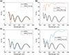 |
Figure 2 Measured reflectance spectra of Si + 800 nm SiO2 stacks with and without an additional absorbing layer, showing the impact of the thinnest and thickest layers of Ag or Au studied in this work: (a) 1 nm Ag; (b) 50 nm Ag; (c) 1 nm Au; and (d) 41 nm Au. For the thinnest layers (a and c), the effect on the reflectance spectrum is significant but small; a thinner layer will produce an even smaller effect, which may harm the accuracy of the fitting. For the thickest layers (b and d), the prominence of the oscillatory fringes is reduced; for thicker layers than this, the fringes are reduced further or even eliminated, which likewise reduces the accuracy of the fitting. |
The lower limit for thickness of the absorbing layer arises due to practical concerns (the minimum thickness which can be deposited with sufficient homogeneity using a given method), as well as theoretical concerns (the minimum thickness at which a sufficiently prominent shift in the reflectance spectrum is obtained). For both Au and Ag, the lower limit was found to be around 1 nm for layers deposited using electron beam evaporation.
The effective upper limit for the thickness of the absorbing layer occurs when the opacity of the layer is sufficient to destroy or significantly reduce the prominence of the interference fringes. At or above such a thickness, the signal-to-noise ratio of the fringes is significantly reduced, and so the performance of this technique approaches that of the two-layer method. The thickness at which this occurs depends on the material under study. In [21], Ti layers of up to 70 nm thickness could be successfully characterised with this method. However, in this work we find the effective upper limit to be 50 nm for Ag and 41 nm for Au, above which (under our deposition conditions) the prominence of the fringes became significantly reduced. For study of thicker layers, an alternative technique may be more appropriate (such as spectroscopic ellipsometry, as used in [1] to obtain the optical constants of Au films between 30 and 200 nm thickness).
2.2 Refractive index models
The refractive index of a material can be modelled as a function of the wavelength or energy of incoming light. In this work, layers were described using a combination of the Modified Drude (MD) model with an oscillator model, either the Forouhi-Bloomer (FB) or Lorentz (L) model [23, 24]. The MD model describes the behaviour of free electrons within a material, and extending it using an oscillator allows the modelling of resonances within the layer, such as from interband transitions or electron confinement effects. This enables a more complete description of thin film metal layers, which typically diverge from the “ideal” case of a bulk metal containing free electrons (as in the MD model).
2.2.1 Modified Drude model
The Drude model calculates the dielectric constant ϵ of a metal by modelling the electrons as free-moving solid spheres [25]. The parameters of the model are ϵ∞, the high-energy dielectric constant; Ed, the plasma energy (= ℏωp where ωp is the plasma frequency); and Eγ, the relaxation energy. Later modifications to the model instead replaced Eγ with an energy-dependent variable Eγ(E) [26, 27], in the so-called “modified” Drude model. This gives the dielectric constant of the material as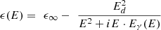 (1)where
  is the energy of incoming light, and
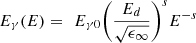 (2)is the energy-dependent relaxation variable. Hence, the MD model has four associated parameters in total: ϵ∞, Ed, Eγ0 and s.
2.2.2 Forouhi-Bloomer model
The Forouhi-Bloomer model [28] calculates the imaginary component k of the refractive index by modelling interband transitions, using three fitting parameters A, B, C, as well as the band gap energy Eg: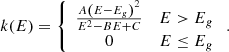 (3)
(3)
The real part n of the refractive index can then be obtained via Kramers-Kronig integration, giving (4)with
![Mathematical equation: $$ {B}_0=\left(A/Q\right)\cdot \left(-\left[{B}^2/2\right]+{E}_gB-{E}_g^2+C\right) $$](/articles/jeos/full_html/2024/01/jeos20230060/jeos20230060-eq6.gif) (5)
(5)
![Mathematical equation: $$ {C}_0=\left(A/Q\right)\cdot \left(\left[{E}_g^2+C\right]B/2-2{E}_gC\right) $$](/articles/jeos/full_html/2024/01/jeos20230060/jeos20230060-eq7.gif) (6)where
(6)where (7)and the high-energy dielectric constant ϵ∞ is shared with the MD model. When using the FB model in combination with the MD model,
  is only added once to the real part of the refractive index. The contributions of j additional interband transitions give additional parameters Aj, Bj and Cj. Hence, the total parameter number for the FB model with j transitions is 3j + 1.
2.2.3 Lorentz oscillator model
The Lorentz oscillator model for refractive index describes electron transitions through one or more Lorentz oscillator terms. When combined with the MD model, the Lorentz contributions are given by a sum of N oscillators [29]: (8)where for the jth oscillator term, fj, ωj and Γj are the oscillator weight, central frequency and damping constant, respectively. Hence, the total parameter number for the Lorentz model with j oscillators is 3j.
2.3 Choice of model
Different materials, or the same material at different thicknesses, are most appropriately described using different models. In this work, the choice whether to use the MD-L or MD-FB model for each layer was made based on how well each model could fit to the measured data, with initial parameters informed by other reports in the literature where possible. During testing, we found that Ag was best described using the combined MD-L model for thinner layers, and the MD-FB model for thicker layers, whereas Au was best described using the MD-FB model only. A maximum of two Lorentz oscillator terms, or one Forouhi-bloomer oscillator term, were used in all calculations, in order to minimise the total number of refractive index parameters (to 10 or 8, respectively) while still enabling an appropriate fit to the measured data.
Finally, the layer thickness was also treated as a free parameter during fitting, in order to find the precise thickness of the deposited layer. The values of layer thickness reported in Sections 3.1 and 3.2 are those obtained during fitting. These values correlate closely with the estimated thickness obtained using a quartz balance during layer deposition.
3 Results
3.1 Silver (Ag)
3.1.1 Refractive index
Ag layers in thicknesses between 1 and 50 nm were deposited in the three-layer configuration with Si and SiO2, and their refractive index was determined by fitting the measured reflectance data to a model. Refractive index plots for the layers studied are shown in Figure 3 for layers 11–50 nm thick, and Figure 4 for “ultrathin” layers below 11 nm thick. For layers above 11 nm thickness, it was found that the MD-L model was most suitable, and for layers below this thickness the MD-FB model was instead used.
 |
Figure 3 Comparison of the determined refractive indices n (left) and k (right) for Ag layers from 11 to 50 nm thickness. As the thickness increases, behaviour in both n and k trend towards the literature values for bulk Ag (long dashed). †: bulk data taken from Johnson and Christy [30]. |
 |
Figure 4 Comparison of the determined refractive indices n (left) and k (right) for Ag layers between 1 and 11 nm thickness. As the thickness decreases towards 1 nm, the material appears to show more dielectric-like behaviour, with a sharp peak in both n and k centered around 0.47 μm and 0.42 μm respectively. |
The results in Figure 3 reveal that the refractive index of the layer changes dramatically as the thickness is reduced. A layer of 30 nm or thicker yields real and imaginary components n and k similar to that of bulk Ag (as reported in [30]). However, as the layer thickness is reduced, k decreases while n increases significantly, both showing a clear oscillatory peak at around 500 nm for n and 410 nm for k. This change is thought to arise from thin-film effects, such as electron confinement or scattering from grain boundaries. The trends observed agree with those reported elsewhere in the literature for Ag thin films, such as in [31].
Ultrathin layers below 11 nm, seen in Figure 4, show a further departure from the index of bulk Ag. The emergence of a sharp peak can be seen in both n and k, growing in prominence as the layer thickness is reduced towards 1 nm. This suggests that the metallic behaviour of the film (described by the Drude model) is minimised for such ultrathin layers, and instead the oscillator-like behaviour (here, described by the Forouhi-Bloomer model) dominates.
In repeatability tests, it was found that samples prepared to the same nominal thickness of Ag yielded the same refractive index to within a maximum of ±0.07 in both n and k, with variations of about ±0.3 nm in determined layer thickness d. This suggests a high precision and confidence for these results.
3.1.2 AFM imaging
To support these results and give more insight into the physical structure of these ultrathin layers, AFM images were acquired in tapping mode for Ag layers of several different thicknesses. More detail on the experimental procedure is given in Section 4.4.
The AFM measurements of these samples reveal a dramatic change in the layer structure and topography as the thickness increases. Figures 5 and 6 show, respectively, the topography and the mechanical phase of silver samples from 1.1 to 50 nm nominal thickness, which reveal that the film structure goes through several different stages: first the formation of discrete nanoparticles; then the coalescence of these particles into a uniform film; and finally the formation of larger and larger grains as the layer thickness increases further.
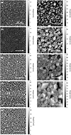 |
Figure 5 AFM topography of Ag samples of various thicknesses. The very thin layers show the formation of discrete nanoparticles on the substrate. As the layer thickness increases, the nanoparticles coalesce into a uniform film, forming grains of increasingly larger sizes. Nominal layer thickness: (a) 1.1 nm, (b) 3.4 nm, (c) 5.7 nm, (d) 7 nm, (e) 11 nm, (f) 14.1 nm, (g) 21 nm, (h) 30 nm and (i) 50 nm. |
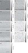 |
Figure 6 AFM mechanical phase measurements of Ag samples of various thicknesses. In (a)–(d), a dark background is seen between the nanoparticles, as they are isolated on the Si + SiO2 substrate. In (e)–(i) (11 nm and above), the dark background cannot be seen, confirming the presence of a continuous layer of Ag with grains formed on top. Nominal layer thickness: (a) 1.1 nm, (b) 3.4 nm, (c) 5.7 nm, (d) 7 nm, (e) 11 nm, (f) 14.1 nm, (g) 21 nm, (h) 30 nm and (i) 50 nm. |
From the layer topography in Figure 5, the evolution in the structure of the layer can be clearly seen. At a layer thickness of 1.1 nm (Fig. 5a), discrete nanoparticles are observed with an average diameter of 37 nm. As the layer thickness increases up to 7 nm, the average diameter of the silver nanoparticles also increases, up to 56 nm. Ag nanoparticles are associated with a strong increase in n and k within the blue/green region, and this is exactly the behaviour seen in the refractive index of these layers (as plotted in Fig. 4). This shows that the optical behaviour of these ultrathin layers is closely linked to the nanostructure of the films.
As the layer thickness increases further to 11 nm (Fig. 5e), coalescence of the Ag nanoparticles and the formation of a continuous silver layer covering the substrate is seen. Hence, a thickness of around 11 nm appears to represent a transition in the layer structure between discrete nanoparticles, and a continuous film made up of grains. This is reflected in the refractive index behaviour of the film, which was found to be equally well-described by either the MD-FB model (associated with ultrathin Ag layers) or the MD-L model (associated with thicker Ag layers whose index converges towards bulk silver).
Following this phase of transition, we can observe the formation and evolution of distinct silver grains. The size of the grains increases with the thickness of the layers, from small grains around 100 nm across in a layer of 14 nm thickness (Fig. 5f) up to grains several hundred nm across in the thickest layer studied of 50 nm (Fig. 5i). This trend in grain size growth agrees with that seen in the literature [32].
In Figure 6, the variation of mechanical phase is shown, which reveals information about the visco-elastic properties of the film. In tapping mode, the AFM cantilever is driven with a sinusoidal force, and can simultaneously record a topographic image and a mechanical phase image. The mechanical phase lag depends on the material properties of the sample, and typically regions with higher viscosity are associated with higher phase lag values within the sample. The mechanical phase images for layers up to 11 nm (Figs. 6a–6e) appear very similar to the topographic images in Figure 5. However, for the thicker layers (Figs. 6f–6i), the topographic images show a dark background in between the grains, whereas the mechanical phase images show a similar phase lag all over the surface. This confirms that the samples show a continuous Ag film, with larger grains on top.
When assessing these AFM images, it is important to note the impact of tip-sample convolution errors, which occur when the region of the AFM tip interacting with the surface is on a similar scale to the features being measured [33]. Tip-sample convolution can cause significant artifacts in the data, such as broadening of measured features [34], and this poses an issue when trying to extract the “real” surface topography.
In these images (as well as the ones presented for Au), the tip-sample convolution has not been corrected. As such, the sizes of the nanoparticles measured here are only relative sizes, and they may not represent the true topography of the surface. However, all of the samples presented were measured on the same day and under the same conditions – the same tip was used, and the tip-sample distance was kept consistent. Therefore, although there may be artefacts in the data causing the profiles shown here to differ from the real topography, the relative trends seen in the evolution of feature size (from small nanoparticles to large grains) are still a valuable qualitative representation of the real surface
A qualitative summary of the layer thickness, structure, and optical behaviour for the Ag samples studied is given in Table 1.
Summary for thin Ag films of changing nanostructure and refractive index behaviour.
3.1.3 Conclusion
A clear correlation is seen between the refractive index behaviour of silver films, and the structure growth of the films as revealed using AFM. Two main regimes of behaviour can be identified. For thin layers (approximately below 11 nm), the film is made of discrete Ag nanoparticles. The refractive index shows corresponding sharp peaks in n and especially k within the blue-green range characteristic of silver nanoparticles, which decrease in height and become redshifted as the nanoparticle size increases with the film thickness. Within this regime, the refractive index behaves according to a combined Modified Drude and Lorentz model.
Above 11 nm, the film coalesces into a uniform layer, and the formation of larger and larger grains can be seen as the thickness increases. This corresponds to the refractive index of the film rapidly approaching that of the bulk material (which typically exhibits grains on the scale of tens or hundreds of microns). These layers are best described with a combined Modified Drude and Forouhi-Bloomer model.
The layer sample of 11 nm appears to occur at approximately the transitional state between the two regimes (under our chosen deposition conditions), where the nanoparticles begin to coalesce into a continuous layer but before the formation of large grains begins. The behaviour of this layer may be described with either a combined Modified Drude and Lorentz model, or a Modified Drude and Forouhi-Bloomer model.
The determined refractive index values for all Ag films shown in the paper are available in spreadsheet form as a Supplementary file.
3.2 Gold (Au)
3.2.1 Refractive index
Au layers between 1.5 nm and 41 nm thickness were prepared in the three-layer configuration using Si and SiO2, and the refractive index of these layers determined by fitting against the measured reflectance data. Plots of refractive index are shown in Figure 7 for layers of 10 nm thickness and above, and Figure 8 for layers of less than 10 nm thickness. For all gold layers studied, it was found that a Modified Drude model with a single Forouhi-Bloomer oscillator term (MD-FB) gave the best match to the data.
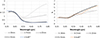 |
Figure 7 Comparison of the determined refractive indices n (left) and k (right) for Au layers from 10 to 41 nm thickness. The 10 nm layer has behaviour markedly different from that of bulk gold. However, as the thickness increases, the refractive index in n and k rapidly converges towards that of the bulk material, reaching an index within 0.2 of that reported in literature for a layer of just 22 nm thickness. *: bulk data taken from the Sopra SA database, currently available at [35]. |
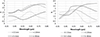 |
Figure 8 Comparison of the determined refractive indices n (left) and k (right) for Au layers between 1.5 and 10 nm thickness. Strongly-varying index behaviour is seen. For the thinnest layer (1.5 nm), the refractive index n appears very low, increasing for slightly thicker layers (2.8 nm and 5.3 nm) before decreasing again for a 10 nm thick layer. The shape of k appears to “flip”, from being strongly absorbing at shorter wavelengths for the 1.5 nm thick layer, to strongly absorbing at longer wavelengths for the thicker layers (in line with the behaviour of bulk Au). |
As with Ag, the behaviour of thin gold layers is seen to be very different to that of the bulk material. However, the index of Au converges towards that of bulk material much more rapidly as the thickness of the layers increases in comparison to Ag. We found a layer of only 22 nm Au yielded a very similar refractive index to bulk Au (as reported in [35]). These trends broadly agree with those reported previously for the indices of gold thin films, such as [31].
The behaviour of ultrathin layers below 10 nm thickness (Fig. 8) shows a large variation in index between layers. For the thinnest layer of 1.5 nm, the real part n of the refractive index is low, with a single isolated peak around 620 nm corresponding roughly with the edge of the absorbance band seen in k. However, for thicker layers of 2.8 and 5.3 nm, two distinct peaks are seen in n, and the shape of k changes significantly, from strongly absorbing shorter wavelengths to longer wavelengths. Finally, when the layer thickness increases further to 10 nm, the shape of n and k changes again, with n reduced to around half its value for the 5.3 nm layer, and the edge in k becoming smoothed out, beginning to approach the shape seen for bulk Au. As was observed for Ag films, the thicker layers yield optical properties similar to that of the bulk material, suggesting that metallic behaviour dominates; whereas the properties of the thinner layers begin to diverge significantly, indicating the metallic behaviour is minimised in favour of other contributions.
3.2.2 AFM imaging
AFM images were acquired in tapping mode for Au samples of three different thicknesses: 2.8 nm, 15 nm and 41 nm. Figure 9 shows the resulting topography (left column) and mechanical phase images (right column) of these samples.
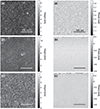 |
Figure 9 AFM topography (left column) and mechanical phase (right column) of Au samples of (a) 2.8 nm, (b) 15 nm and (c) 41 nm thickness. The 2.8 nm layers show discrete gold nanoparticles on the substrate. At 15 nm, these particles coalesce into a uniform layer showing distinct grains, and when the layer thickness further increases to 41 nm the grain size likewise increases. |
At 2.8 nm, the layer is composed of discrete gold nanoparticles with an average diameter of 40 nm. The mechanical phase recorded for this layer shows a significant phase contrast, confirming that the gold nanoparticles are not uniformly covering the silica substrate. The 15 nm film shows the coalescence of the nanoparticles, and the formation of gold grains within the layer, similar to the behaviour of the silver nanoparticles. Finally, the 41 nm thick sample shows a continuous layer, with even larger grains and a highly uniform mechanical phase (Δϕ = 0.304 rad), indicating that the layer is exhibiting similar behaviour to bulk Au.
Table 2 shows a summary of the changing nanostructure of the thin films as the thickness increases, and the corresponding refractive index behaviour. As with Ag, the nanostructure of the layer changes as the thickness increases, from nanoparticles to small and then larger grains. This changing structure correlates with the refractive index determined by the earlier analysis.
Summary for thin Au films of changing nanostructure and refractive index behaviour.
Notably, the scale of the grain in the Au films is much smaller than those in the Ag films. Ag is known to exhibit grains on the scale of hundreds of nm up to or even, whereas the grain size in the Au films studied had a maximum observed grain size of ∼40 nm. This may indicate why the index of the thin Au films converges much more rapidly to that of the bulk material than thin Ag films.
3.2.3 Conclusion
The refractive index of the Au samples, combined with the AFM images, show a clear trend in behaviour from the thicker layers (for which the refractive index is similar to that of bulk Au) to the thinnest layers (for which the refractive index diverges wildly). Below ∼10–15 nm, the deposited film forms small, discrete nanoparticles on the surface. The corresponding refractive index of these layers shows sharp peaks, relating to the well-known absorption peak of gold nanoparticles. As the layer thickness increases from 1.5 nm to 5.3 nm, redshifting occurs of the oscillations in n, suggesting that the size of the gold nanoparticles likewise increases (similarly to the trend observed in Ag films).
As well as resonant absorption from Au nanoparticles, reports from the literature suggest there may be other complex physical phenomena contributing to the significant variation in the optical properties of ultrathin gold films. Yakubovsky et al. [1] report that the behaviour of gold films of 20 nm and above also depends on grain-boundary scattering, where the grain size varies nonlinearly with the film thickness. Qian et al. [4] show that for ultrathin gold films around 2.5 nm thickness, the optical behaviour diverges significantly, which they propose as being influenced by quantum well confinement effects. A full investigation of these phenomena is outside the scope of this work; however, such reports, alongside the variation in nanostructure revealed by the AFM images, may indicate that the dramatic variation observed in refractive index for different thicknesses of Au films is influenced by several complex physical factors. This result also further emphasizes the importance of robust techniques for characterisation of these films, as the variation in refractive index with film thickness will no doubt also depend on the deposition technique and conditions.
Above 10–15 nm, the thin film coalesces into a uniform layer. The refractive index behaviour is seen to converge rapidly towards that of bulk gold as the thickness increases. In addition, the mechanical phase AFM images show that the layer is very homogeneous, and the local roughness scale is much lower than was observed for Ag films, which may both be contributing factors to the faster convergence towards the index of bulk material.
The determined refractive index values for all Au films shown in the paper are available in spreadsheet form as a Supplementary file.
4 Experimental methods
4.1 Deposition of thin-film coatings
The thin film layers in this work were deposited using electron beam evaporation in a Bühler-Leybold Optics SYRUSpro vacuum deposition machine. Depositions were carried out under a vacuum of around 5 × 10⁻⁷ mbars, at a rate of approximately 1 nm/s for SiO2 layers and 0.1 nm/s for metal layers. The substrates used were commercial Si wafers.
4.2 Spectrophotometric measurements
The reflectance of deposited samples was measured using a Perkin-Elmer Lambda1050 spectrophotometer, between 370 and 835 nm. Measurements were taken at 8°, as close to normal incidence as possible.
4.3 Refractive index optimisation
Optimization of refractive index against measured data was performed in MATLAB, using the inbuilt global optimization algorithms from MATLAB’s global optimization toolbox. For more information, see [36].
4.4 AFM measurements
To perform the AFM characterization of Ag and Au films, we used a commercially available VIS-neaSCOPE in the AFM mode. We chose to work in AFM tapping-mode, allowing us to record the topography, the mechanical amplitude and the mechanical phase of the studied sample. For this study, the same tip was used to characterize all the samples: a NanoWorld® ArrowTM NCPt probe with a radius of curvature around 20 nm. Scans were made on a 1.5 × 1.5 μm2 surface, with a definition of 300 × 300 pixel2 and an integration time of 7 ms per pixel. For image processing, the software Gwyddion [37] was used to remove sample tilt, set the minimum value to zero (for the topography images only) and adjust the contrast of the image. This same postprocessing approach was used for all AFM images shown in this paper.
Supplementary material
Supplementary file: The determined refractive index information for the Ag and Au layers described in this paper is available in spreadsheet form. Access Supplementary Material
Funding
This research did not receive any specific funding.
Conflicts of Interest
The authors declare that they have no competing interests.
Data availability statement
The refractive index data shown in the paper is available in a supplementary file. Raw measurement data is available from the authors on request.
Author contribution statement
R. Shurvinton wrote most of the manuscript, fabricated the samples, and performed refractive index characterisation. V. Allard provided the AFM images, and wrote the experimental section on AFM and the analysis of the AFM images along with F. Lemarchand. A. Lereu wrote the theory and analysis of the AFM images. All authors contributed to proofreading and editing the manuscript.
References
- Yakubovsky D.I., Arsenin A.V., Stebunov Y.V., Fedyanin D.Y., Volkov V.S. (2017) Optical constants and structural properties of thin gold films, Opt. Express 25, 21, 25574–25587. https://doi.org/10.1364/OE.25.025574. [NASA ADS] [CrossRef] [Google Scholar]
- Mayadas A.F., Shatzkes M., Janak J.F. (1969) Electrical resistivity model for polycrystalline films: The case of specular reflection at external surfaces, Appl. Phys. Lett. 14, 11, 345–347. https://doi.org/10.1063/1.1652680. [NASA ADS] [CrossRef] [Google Scholar]
- Mayadas A.F., Shatzkes M. (1970) Electrical-resistivity model for polycrystalline films: the case of arbitrary reflection at external surfaces, Phys. Rev. B 1, 1382–1389. https://doi.org/10.1103/PhysRevB.1.1382. [NASA ADS] [CrossRef] [Google Scholar]
- Qian H., Xiao Y., Lepage D., Chen L., Liu Z. (2015) Quantum electrostatic model for optical properties of nanoscale gold films, Nanophotonics 4, 4, 413–418. https://doi.org/10.1515/nanoph-2015-0022. [Google Scholar]
- Li X.D., Chen T.P., Liu Y., Leong K.C. (2015) Evolution of the localized surface plasmon resonance and electron confinement effect with the film thickness in ultrathin Au films, J. Nanoparticle Res. 17, 2, 67. https://doi.org/10.1007/s11051-015-2880-1. [NASA ADS] [CrossRef] [Google Scholar]
- Reddy H., Guler U., Kildishev A.V., Boltasseva A., Shalaev V.M. (2016) Temperature-dependent optical properties of gold thin films, Opt. Mater. Express 6, 9, 2776–2802. https://doi.org/10.1364/OME.6.002776. [Google Scholar]
- Berning P.H., Turner A.F. (1957) Induced transmission in absorbing films applied to band pass filter design, J. Opt. Soc. Am. 47, 3, 230–239. https://doi.org/10.1364/JOSA.47.000230. [NASA ADS] [CrossRef] [Google Scholar]
- Dobrowolski J.A., Li L., Kemp R.A. (1995) Metal/dielectric transmission interference filters with low reflectance. 1. Design, Appl. Opt. 34, 25, 5673–5683. https://doi.org/10.1364/AO.34.005673. [NASA ADS] [CrossRef] [Google Scholar]
- Zheng Y., Kikuchi K., Yamasaki M., Sonoi K., Uehara K. (1997) Two-layer wideband antireflection coatings with an absorbing layer, Appl. Opt. 36, 25, 6335–6338. https://doi.org/10.1364/AO.36.006335. [NASA ADS] [CrossRef] [Google Scholar]
- Lemarquis F., Marchand G. (1999) Analytical achromatic design of metal-dielectric absorbers, Appl. Opt. 38, 22, 4876–4884. https://doi.org/10.1364/AO.38.004876. [NASA ADS] [CrossRef] [Google Scholar]
- Fang Y., Sun M. (2015) Nanoplasmonic waveguides: towards applications in integrated nanophotonic circuits, Light Sci. Appl. 4, 6, 294–294. https://doi.org/10.1038/lsa.2015.67. [Google Scholar]
- Andam N., Refki S., Hayashi S., Sekkat Z. (2021) Plasmonic mode coupling and thin film sensing in metal-insulator-metal structures, Sci. Rep. 11, 1, 15093. https://doi.org/10.1038/s41598-021-94143-2. [CrossRef] [Google Scholar]
- Ghosh D.S., Martinez L., Giurgola S., Vergani P., Pruneri V. (2009) Widely transparent electrodes based on ultrathin metals, Optics Letters 34, 3, 325–327. https://doi.org/10.1364/OL.34.000325. [NASA ADS] [CrossRef] [Google Scholar]
- Bi Y.-G., Liu Y.-F., Zhang X.-L., Yin D., Wang W.-Q., Feng J., Sun H.-B. (2019) Ultrathin metal films as the transparent electrode in ITO-free organic optoelectronic devices, Adv. Opt. Mater. 7, 6, 1800778. https://doi.org/10.1002/adom.201800778. [CrossRef] [Google Scholar]
- Ji C., Liu D., Zhang C., Jay Guo L. (2020) Ultrathin-metal-film-based transparent electrodes with relative transmittance surpassing 100%, Nat. Commun. 11, 1, 3367. https://doi.org/10.1038/s41467-020-17107-6. [Google Scholar]
- Phillips R.W., Bleikolm A.F. (1996) Optical coatings for document security, Appl. Opt. 35, 28, 5529–5534. https://doi.org/10.1364/AO.35.005529. [NASA ADS] [CrossRef] [Google Scholar]
- Baloukas B., Trottier-Lapointe W., Martinu L. (2014) Fabry-Perot-like interference security image structures: From passive to active, Solid Films 559, 9–13. https://doi.org/10.1016/j.tsf.2013.10.030. [CrossRef] [Google Scholar]
- Wang D., Liu Z., Wang H., Li M., Guo L.J., Zhang C. (2023) Structural color generation: from layered thin films to optical metasurfaces, Nanophotonics 12, 6, 1019–1081. https://doi.org/10.1515/nanoph-2022-0063. [Google Scholar]
- Swanepoel R. (1983) Determination of the thickness and optical constants of amorphous silicon, J. Phys. E Sci. Instr. 16, 12, 1214–1222. https://doi.org/10.1088/0022-3735/16/12/023. [NASA ADS] [CrossRef] [Google Scholar]
- Poelman D., Smet P.F. (2003) Methods for the determination of the optical constants of thin films from single transmission measurements: a critical review, J. Phys. D Appl. Phys. 36, 1850–1857. [NASA ADS] [CrossRef] [Google Scholar]
- Shurvinton R., Lemarchand F., Moreau A., Lumeau J. (2021) Precise spectrophotometric method for semitransparent metallic thin-film index determination using interference enhancement, J. Eur. Opt. Soc. Rapid Publ. 17, 1, 29. https://doi.org/10.1186/s41476-021-00172-9. [CrossRef] [Google Scholar]
- Nestler P., Helm C.A. (2017) Determination of refractive index and layer thickness of nm-thin films via ellipsometry, Opt. Express 25, 22, 27077–27085. https://doi.org/10.1364/OE.25.027077. [NASA ADS] [CrossRef] [Google Scholar]
- Lai F., Lin L., Gai R., Lin Y., Huang Z. (2007) Determination of optical constants and thicknesses of In2O3:Sn films from transmittance data, Thin Solid Films 515, 18, 7387–7392. [NASA ADS] [CrossRef] [Google Scholar]
- Barchiesi D., Grosges T. (2014) Fitting the optical constants of gold, silver, chromium, titanium, and aluminum in the visible bandwidth, J. Nanophotonics 8, 1, 1–17. https://doi.org/10.1117/1.JNP.8.083097. [NASA ADS] [CrossRef] [Google Scholar]
- Drude P. (1902) Zur Elektronentheorie der metalle. Ann. Phys. 312, 3, 687–692. https://doi.org/10.1002/andp.19023120312. [NASA ADS] [CrossRef] [Google Scholar]
- Hamberg I., Granqvist C.G. (1986) Evaporated sn-doped in2o3 films: Basic optical properties and applications to energyefficient windows, J. Appl. Phys. 60, 123–160. [Google Scholar]
- Ederth J., Johnsson P., Niklasson G.A., Hoel A., Hultåker A., Heszler P., Granqvist C.G., van Doorn A.R., Jongerius M.J., Burgard D. (2003) Electrical and optical properties of thin films consisting of tin-doped indium oxide nanoparticles, Phys. Rev. B 68, 155410. https://doi.org/10.1103/PhysRevB.68.155410. [CrossRef] [Google Scholar]
- Forouhi A.R., Bloomer I. (1988) Optical properties of crystalline semiconductors and dielectrics, Phys. Rev. B 38, 3, 1865–1874. [CrossRef] [Google Scholar]
- Rakić A.D., Djurišić A.B., Elazar J.M., Majewski M.L. (1998) Optical properties of metallic films for vertical-cavity optoelectronic devices, Appl. Opt. 37, 22, 5271–5283. https://doi.org/10.1364/AO.37.005271. [CrossRef] [Google Scholar]
- Johnson P.B., Christy R.W. (1972) Optical constants of the noble metals, Phys. Rev. B 6, 4370–4379. https://doi.org/10.1103/PhysRevB.6.4370. [CrossRef] [Google Scholar]
- Kim J., Oh H., Seo M., Lee M. (2019) Generation of reflection colors from metal-insulator-metal cavity structure enabled by thickness-dependent refractive indices of metal thin film, ACS Photonics 6, 9, 2342–2349. https://doi.org/10.1021/acsphotonics.9b00894. [CrossRef] [Google Scholar]
- Shiva L.U., Ayachit N.H., Udachan L.A. (2019) Electrical and microstructural properties of silver thin films, Int. J. Nanoelectron. Mater. 12, 2, 221–236. [NASA ADS] [Google Scholar]
- Schwarz U.D., Haefke H., Reimann P., Güntherodt H.-J. (1994) Tip artefacts in scanning force microscopy, J. Microsc. 173, 3, 183–197. https://doi.org/10.1111/j.1365-2818.1994.tb03441.x. [CrossRef] [Google Scholar]
- Shen J., Zhang D., Zhang F.-H., Gan Y. (2017) AFM tip-sample convolution effects for cylinder protrusions, Appl. Surf. Sci. 422, 482–491. https://doi.org/10.1016/j.apsusc.2017.06.053. [CrossRef] [Google Scholar]
- Sopra SA refractive index database. Available at http://www.sspectra.com/sopra.html (accessed November 24, 2022). [Google Scholar]
- MATLAB Documentation – GlobalSearch. Available at https://www.mathworks.com/help/gads/globalsearch.html (accessed November 14, 2022). [Google Scholar]
- Nečas D., Klapetek P. (2012) Gwyddion: an open-source software for SPM data analysis, Cent. Eur. J. Phys. 10, 181–188. https://doi.org/10.2478/s11534-011-0096-2. [Google Scholar]
All Tables
Summary for thin Ag films of changing nanostructure and refractive index behaviour.
Summary for thin Au films of changing nanostructure and refractive index behaviour.
All Figures
|
Figure 1 (a) Simulated reflectance and transmittance of a B270 glass slide, with and without a 1 nm thick Ag-like layer. Only a very small change in both R and T are observed. (b) Simulated reflectance of a stack with opaque Si + 800 nm SiO2, with and without a 1 nm thick Ag-like layer. Compared to (a), a much more dramatic shift in the reflectance spectrum is seen when the Ag layer is added. |
| In the text | |
|
Figure 2 Measured reflectance spectra of Si + 800 nm SiO2 stacks with and without an additional absorbing layer, showing the impact of the thinnest and thickest layers of Ag or Au studied in this work: (a) 1 nm Ag; (b) 50 nm Ag; (c) 1 nm Au; and (d) 41 nm Au. For the thinnest layers (a and c), the effect on the reflectance spectrum is significant but small; a thinner layer will produce an even smaller effect, which may harm the accuracy of the fitting. For the thickest layers (b and d), the prominence of the oscillatory fringes is reduced; for thicker layers than this, the fringes are reduced further or even eliminated, which likewise reduces the accuracy of the fitting. |
| In the text | |
|
Figure 3 Comparison of the determined refractive indices n (left) and k (right) for Ag layers from 11 to 50 nm thickness. As the thickness increases, behaviour in both n and k trend towards the literature values for bulk Ag (long dashed). †: bulk data taken from Johnson and Christy [30]. |
| In the text | |
|
Figure 4 Comparison of the determined refractive indices n (left) and k (right) for Ag layers between 1 and 11 nm thickness. As the thickness decreases towards 1 nm, the material appears to show more dielectric-like behaviour, with a sharp peak in both n and k centered around 0.47 μm and 0.42 μm respectively. |
| In the text | |
|
Figure 5 AFM topography of Ag samples of various thicknesses. The very thin layers show the formation of discrete nanoparticles on the substrate. As the layer thickness increases, the nanoparticles coalesce into a uniform film, forming grains of increasingly larger sizes. Nominal layer thickness: (a) 1.1 nm, (b) 3.4 nm, (c) 5.7 nm, (d) 7 nm, (e) 11 nm, (f) 14.1 nm, (g) 21 nm, (h) 30 nm and (i) 50 nm. |
| In the text | |
|
Figure 6 AFM mechanical phase measurements of Ag samples of various thicknesses. In (a)–(d), a dark background is seen between the nanoparticles, as they are isolated on the Si + SiO2 substrate. In (e)–(i) (11 nm and above), the dark background cannot be seen, confirming the presence of a continuous layer of Ag with grains formed on top. Nominal layer thickness: (a) 1.1 nm, (b) 3.4 nm, (c) 5.7 nm, (d) 7 nm, (e) 11 nm, (f) 14.1 nm, (g) 21 nm, (h) 30 nm and (i) 50 nm. |
| In the text | |
|
Figure 7 Comparison of the determined refractive indices n (left) and k (right) for Au layers from 10 to 41 nm thickness. The 10 nm layer has behaviour markedly different from that of bulk gold. However, as the thickness increases, the refractive index in n and k rapidly converges towards that of the bulk material, reaching an index within 0.2 of that reported in literature for a layer of just 22 nm thickness. *: bulk data taken from the Sopra SA database, currently available at [35]. |
| In the text | |
|
Figure 8 Comparison of the determined refractive indices n (left) and k (right) for Au layers between 1.5 and 10 nm thickness. Strongly-varying index behaviour is seen. For the thinnest layer (1.5 nm), the refractive index n appears very low, increasing for slightly thicker layers (2.8 nm and 5.3 nm) before decreasing again for a 10 nm thick layer. The shape of k appears to “flip”, from being strongly absorbing at shorter wavelengths for the 1.5 nm thick layer, to strongly absorbing at longer wavelengths for the thicker layers (in line with the behaviour of bulk Au). |
| In the text | |
|
Figure 9 AFM topography (left column) and mechanical phase (right column) of Au samples of (a) 2.8 nm, (b) 15 nm and (c) 41 nm thickness. The 2.8 nm layers show discrete gold nanoparticles on the substrate. At 15 nm, these particles coalesce into a uniform layer showing distinct grains, and when the layer thickness further increases to 41 nm the grain size likewise increases. |
| In the text | |
Current usage metrics show cumulative count of Article Views (full-text article views including HTML views, PDF and ePub downloads, according to the available data) and Abstracts Views on Vision4Press platform.
Data correspond to usage on the plateform after 2015. The current usage metrics is available 48-96 hours after online publication and is updated daily on week days.
Initial download of the metrics may take a while.