| Issue |
J. Eur. Opt. Society-Rapid Publ.
Volume 22, Number 1, 2026
EOSAM 2025
|
|
|---|---|---|
| Article Number | 29 | |
| Number of page(s) | 9 | |
| DOI | https://doi.org/10.1051/jeos/2026030 | |
| Published online | 24 April 2026 | |
Review Article
Evaluation of surface topography and microstructure of electroplated copper ultraprecision-machined with a single-crystal diamond tool
1
Chiba Institute of Technology, Narashino, Chiba 275-0016, Japan
2
Sendai Nikon Corporation, Natori, Miyagi 981-1221, Japan
3
JTEC Corporation, Ibaraki, Osaka 567-0086, Japan
* Corresponding author: This email address is being protected from spambots. You need JavaScript enabled to view it.
, This email address is being protected from spambots. You need JavaScript enabled to view it.
Received:
3
December
2025
Accepted:
14
March
2026
Abstract
We investigated in detail the surface characteristics of ultraprecision-machined electroplated copper (Cu). Electroplated Cu, as well as electroless-plated nickel phosphorus (NiP) and oxygen-free copper (OFC) for comparison, was machined using an ultraprecision turning machine with a single-crystal diamond tool. The resulting surfaces were measured over an area of 140 μm × 105 μm by white-light interferometry, revealing that the electroplated Cu surface exhibited the lowest surface roughness of 0.83 nm root-mean-square (RMS) among the three materials. For a smaller area of 1 μm × 1 μm measured by atomic force microscopy, the electroplated Cu surface exhibited a sand-like texture with a surface roughness of 1.74 nm RMS. Power spectral density (PSD) analysis revealed that the electroplated Cu surface had a lower PSD than the OFC surface below a spatial frequency of 2 × 104 mm−1 and was comparable to the electroless-plated NiP surface below a spatial frequency of 1 × 103 mm−1. Electron backscatter diffraction and X-ray diffraction analyses indicated that the electroplated Cu was composed of fine crystalline microstructures, which was probably the reason for the sand-like texture. Overall, the electroplated Cu surface exhibited excellent smoothness and machinability, superior to the OFC surface and close to electroless-plated NiP surface, demonstrating its suitability for ultraprecision optical components.
Key words: Surface / Machining / Diamond turning / Electroplated Cu / Electroless-plated NiP / Oxygen-free copper
© The Author(s), published by EDP Sciences, 2026
 This is an Open Access article distributed under the terms of the Creative Commons Attribution License (https://creativecommons.org/licenses/by/4.0), which permits unrestricted use, distribution, and reproduction in any medium, provided the original work is properly cited.
1 Introduction
In optical fabrication, an ultraprecision machine tool with a single-crystal diamond tool is effectively used to obtain smooth and highly accurate metal surfaces for optical components, such as those of mirrors and injection molds [1, 2]. Electroless-plated nickel phosphorus (NiP) is a widely used material for single-crystal diamond machining to achieve a smooth surface [3–14]. However, the major issues in machining electroless-plated NiP are tool wear and chipping [4, 5, 7–10, 13, 14].
To overcome this problem, alternative materials that can achieve smooth optical surfaces with lower tool wear are desirable. Because copper is softer than electroless-plated NiP, machining copper may help reduce the wear and chipping of the diamond tool. Oxygen-free copper (OFC) is one candidate material because it can be machined with a single-crystal diamond tool [15–22]. However, the machined surface of OFC often exhibits irregularities owing to crystal grains, resulting in an increase in surface roughness [15, 16, 18, 19, 21]. Although OFC has high thermal conductivity and is suitable for optical components subjected to high thermal loads when adequate cooling is applied, these surface irregularities can affect the surface quality when extremely smooth optical surfaces are required. Therefore, it is important to investigate alternative copper-based materials that can maintain the advantages of OFC while enabling the formation of smoother optical surfaces by ultraprecision diamond machining.
Electroplated copper (Cu) is therefore expected to be a promising alternative material for optical components. Because electroplated Cu generally has finer grains than OFC, it may enable the formation of smoother optical surfaces. In addition, electroplated Cu is also softer than electroless-plated NiP and is therefore expected to reduce tool wear and chipping during diamond machining. Furthermore, when a copper electroplating layer is applied to the surface of OFC, it may enable the fabrication of optical components that combine extremely smooth optical surfaces with high thermal conductivity.
In our previous studies [23, 24], we demonstrated the successful fabricating of mirror arrays with high shape accuracy using an ultraprecision milling machine with a single-crystal diamond tool. In the machining, a mirror surface was formed on a 1-mm-thick electroplated Cu layer on a block, allowing the mirror array to be machined into the thick copper layer. The reason for the use of electroplated Cu was that it is considered to cause less tool wear and chipping than electroless-plated NiP. Moreover, we expected that the grain size of electroplated Cu would likely be smaller than that of OFC, providing smooth surfaces without irregularities. In our previous studies, we focused on the shape accuracy of the electroplated Cu surface in ultraprecision milling, and we have not studied the roughness of the machined surface in detail.
For optical components, the surface roughness after machining is a critical factor because it directly affects optical performance. To the best of our knowledge, the surface characteristics of electroplated Cu after ultraprecision diamond machining have not yet been fully clarified [23–31]. Understanding these surface characteristics is important for the design and fabrication of high-performance optical components. Therefore, the objective of this study is to clarify the surface roughness characteristics of electroplated Cu after ultraprecision machining and to compare them with those of OFC and electroless-plated NiP.
To achieve this objective, the surfaces of electroplated Cu, OFC, and electroless-plated NiP were machined by ultraprecision turning with a single-crystal diamond tool, and the resulting surface roughnesses in areas of 140 μm × 105 μm and 1 μm × 1 μm were evaluated. Moreover, the microstructure of the machined surfaces was analyzed by electron backscatter diffraction (EBSD) and X-ray diffraction (XRD) to investigate the relationship between the microstructure and the surface topography. This study provides insight into the feasibility of electroplated Cu as an alternative material for ultraprecision optical fabrication.
2 Experimental methods
The electroplated Cu specimens and the OFC specimens were cylinders with a diameter of 20 mm and a height of 10 mm. The NiP-electroless-plated specimens were cylinders with a diameter of 20 mm and a height of 7 mm. Cu plating and NiP plating were carried out by Kyowa Sangyo Corporation, Japan. The thicknesses of the electroplated Cu and electroless-plated NiP were approximately 0.2 and 0.1 mm, respectively. The substrates for the electroplated Cu and the electroless-plated NiP were OFC and stainless-steel cylinders, respectively. Cu electroplating was carried out using a plating solution in which Cu sulfate served as the main constituent. Electroless-plated NiP used in this study had a phosphorus concentration of approximately 11%.
The face of the specimens was turned with an ultraprecision turning machine with a single-crystal diamond tool having a nose radius of 0.5 mm. First, all specimens were roughly turned. After replacing the rough-turning tool with a new one, finish turning was performed using the same tool for all materials. The finishing process was performed sequentially on the OFC, electroplated Cu, and electroless-plated NiP so that electroless-plated NiP, which was considered most likely to cause tool damage, was machined last. The depth of cut was set to 5 and 2 μm in the rough and finishing processes, respectively. The tool feed rate was 2 mm/min, and the spindle speed was 1000 rpm for each process. At these tool feed rate and spindle speed, the distance between tool marks is calculated to be 2 μm.
After turning, the surface topographies of the machined surfaces were measured using a white-light interferometer (WLI) (Zygo, NewView 7300) and an atomic force microscope (AFM) (Shimazu, SPM-9700HT). In the measurement using the WLI, an area of 140 μm × 105 μm was measured with a horizontal resolution of 220 nm. In the measurement using the AFM, an area of 1 μm × 1 μm was measured with a horizontal resolution of 4 nm. Both measurements were performed at approximately the midpoint in the radial direction of the workpiece, 5 mm from the center. Moreover, the microstructure of the machined surfaces was analyzed by XRD (Rigaku, SmartLab) and EBSD (Oxford Instruments, Symmetry). XRD analysis was performed using the in-plane method. This method enables the investigation of the surface structure by limiting X-ray penetration through grazing incidence.
3 Results and discussion
3.1 Machined surface topography
Figure 1 shows the topographies of the machined surfaces measured using the WLI. Figures 1a–1c correspond to the topographies of the OFC, electroplated Cu, and electroless-plated NiP surfaces, respectively. As shown in Figure 1a, the OFC surface shows steps, which probably result from crystal grains. In Figure 1a, the height of the step through the center of the measured area is approximately 5 nm, and measurements performed at several other locations also revealed step structures showing comparable overall morphology with minor variations in contour and height. The root-mean-square (RMS) roughness of the OFC surface was 1.78 nm. As shown in Figure 1b, the electroplated Cu surface shows no steps. The RMS roughness of the electroplated Cu surface was 0.87 nm, showing a smoother surface than the OFC surface. As shown in Figure 1c, the electroless-plated NiP surface also shows no step structures, but two hills can be observed with an amplitude of approximately 3 nm and an interval of approximately 90 μm. The RMS roughness of the electroless-plated NiP surface was 1.21 nm. Since similar hills were observed in measurements at several locations, it is considered that concentric waves with a pitch of approximately 90 μm were generated on the surface. Referring again to the electroplated Cu surface shown in Figure 1b, high regions can be observed at approximately 90 μm intervals, although they are less distinct than those on the electroless-plated NiP surface. This reduced clarity may be attributed to the softness of the electroplated Cu, which could have caused deformation during machining. For the OFC surface shown in Figure 1a, it is likely that the large step structures make it difficult to observe the hills. Although not shown here, the hills can be observed on the OFC surface when the step height is small. From these results, it is inferred that these hills, i.e., the wavinesses, were not caused by the material properties but by the motion error of the ultraprecision turning machine.
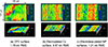 |
Fig. 1 Surface topographies measured with a WLI. |
In addition, measurements were performed at three different locations near the radial midpoint of each workpiece, and the average, maximum, and minimum RMS roughness were obtained. The average, maximum, and minimum RMS roughness were 1.65, 1.78, and 1.52 nm for OFC; 0.83, 0.87, and 0.77 nm for electroplated Cu; and 1.26, 1.30, and 1.21 nm for electroless-plated NiP, respectively. The relatively large range between the maximum and minimum values for OFC is attributed to variations in the contour and height of the crystal grain boundary steps. Thus, the relative magnitudes of the average RMS roughness values obtained from multiple measurements were consistent with those shown in Figure 1.
Next, the surface topographies within an area of 1 μm × 1 μm were measured with the AFM. Figure 2 shows the measurement results, including the surface topographies together with cross-sectional profiles approximately through their centers. The OFC surface had tiny holes, as shown in Figure 2a, whereas the electroplated Cu surface had a sand-textured finish, as shown in Figure 2b. The RMS roughness of the electroplated Cu surface was smaller than that of the OFC surface, that is, 1.72 nm and 2.32 nm, respectively. Compared with these surfaces, the electroless-plated NiP surface was smoother, as shown in Figure 2c. For the electroless-plated NiP surface, the RMS roughness was 1.50 nm. In Figure 2c, small elevations (white dots) are observed scattered on the surface. These are considered to be fine chips generated during turning adhered to the surface. After turning, the surface was only rinsed with an organic solvent using a wash bottle without wiping, in order to preserve the surface morphology as much as possible. As a result, some fine chips likely remained on the machined surface. Thus, although each machined surface exhibited a different surface appearance, the electroplated Cu surface was not as smooth as the electroless-plated NiP surface but was smoother than the OFC surface when uniformly compared in terms of RMS roughness.
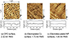 |
Fig. 2 Surface topographies measured with an AFM. |
Figure 3 shows the AFM measurement result for a 10 μm × 10 μm area of the electroless-plated NiP surface machined last. Regular tool marks are observed, and each tool mark exhibits a profile corresponding to the arc of the tool tip. These observations indicate that the original geometry of the cutting edge was almost maintained during the finishing process, suggesting that no significant tool wear or chipping occurred.
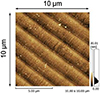 |
Fig. 3 Surface topography measured with an AFM: measurement result for a 10 μm × 10 μm area of the electroless-plated NiP cut surface. |
In addition, measurements were performed at three different locations near the radial midpoint for each material. The average, maximum, and minimum RMS roughness were 2.29, 2.32, and 2.27 nm for OFC; 1.74, 1.77, and 1.72 nm for electroplated Cu; and 1.44, 1.50, and 1.36 nm for electroless-plated NiP, respectively. Thus, the relative magnitudes of the average RMS roughness values obtained from multiple measurements were consistent with those shown in Figure 2.
3.2 Power spectral density (PSD) analysis
We performed the PSD analysis of the obtained surface profiles. Figure 4 shows the PSD curves calculated from the surface profiles measured with the WLI. Specifically, the one-dimensional (1D) PSD curve obtained by WLI was calculated using the software built into the measurement system. The PSD was calculated from a line profile extracted from the center of the measured surface, and the analysis was performed over the full evaluation length of the profile. The PSD curve shown represents the average of three measurements for each material.
 |
Fig. 4 PSD curves calculated from topographies of various machined surfaces measured with a WLI. |
As shown in Figure 3, the PSD of the OFC surface tends to be the highest among the three materials, whereas those of the electroplated Cu and electroless-plated NiP surfaces are similarly low. Thus, the electroplated Cu and electroless-plated NiP surfaces exhibited comparable smoothness and were smoother than the OFC surface. Furthermore, the electroplated Cu and electroless-plated NiP surfaces exhibited similar spatial frequency characteristics over the entire frequency range.
In the previous section, we described that the electroplated Cu and electroless-plated NiP surfaces exhibited hills at intervals of approximately 90 μm. Although the peaks corresponding to these hills exist, the peaks do not appear in the PSD curves because they must be located in the low-frequency region outside the plotted range. However, it is possible that the increase at the left end of the PSD curve of the electroless-plated NiP surface is related to the presence of these hills. Moreover, Figure 4 shows that each PSD curve exhibits a similar sharp peak at a spatial frequency of approximately 5.0 × 103 mm−1. This corresponds to a tool-mark interval of about 2 μm attributed to turning.
Figure 5 shows the PSD curves calculated from the surface profiles measured with the AFM. Similarly, the one-dimensional (1D) PSD curves obtained from the AFM measurements were calculated using in-house software. The software calculates the PSD for all cross-sectional profiles across the measured surface, and the analysis was performed over the full evaluation length of each profile. The PSD curves shown in the figure represent the average of these profiles and correspond to the surface data of the measured area shown in Figure 2. The PSD of the OFC surface was the highest among all materials at spatial frequencies below 1 × 104 mm−1, likely attributable to the presence of the tiny holes on the surface. For the OFC surface, the high PSD in the low-frequency region below 1 × 104 mm−1 is considered to result in the largest RMS value among the three materials. On the other hand, the PSD of the electroplated Cu surface was the highest among all materials at spatial frequencies above 2 × 104 mm−1, which is considered to result from the sand-like texture appearing on the surface.
 |
Fig. 5 PSD curves calculated from topographies of various machined surfaces measured with an AFM. |
Overall, from the PSD analysis results shown in Figures 4 and 5, it can be concluded that the PSD of the electroplated Cu surface is lower than that of the OFC surface at spatial frequencies below 2 × 104 mm−1. Furthermore, at spatial frequencies below 1 × 103 mm−1, the PSD of the electroplated Cu surface is as low as that of the electroless-plated NiP surface, indicating comparable surface quality.
3.3 Material microstructural analysis
The microstructure of the machined electroplated Cu was analyzed by EBSD. This analysis was carried out on the machined surfaces without post-treatments such as polishing and etching, because the machined electroplated Cu was smooth enough for analysis. Figure 6 shows the results of the EBSD analysis, in which (a) the grain map over an area of 6 μm × 6 μm and (b) its grain size distribution histogram are shown. EBSD data were analyzed by defining misorientations exceeding 5° as grain boundaries. The measurements were conducted by scanning an electron beam at a pitch of 20 nm, and the lower detection limit of the EBSD instrument was 40 nm. Thus, fine grains with sizes ranging from 40 to 280 nm were detected on the electroplated Cu. The black areas in Figure 6a are considered to correspond to either micro-grains smaller than 40 nm or amorphous regions.
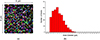 |
Fig. 6 Results of EBSD analysis of the machined electroplated Cu surface. (a) Grain map and (b) grain size distribution histogram. |
Next, the microstructure of the machined electroplated Cu surface was analyzed by XRD. The electroless-plated NiP surface was also analyzed as a reference for comparison; in general, the electroless-plated NiP with a phosphorus concentration of 11% is amorphous [32, 33]. The XRD analysis was also carried out for the machined surfaces without post-treatments. Figures 7a and 7b show the XRD profiles of the electroless-plated NiP and electroplated Cu surfaces, respectively. In Figure 7a, the XRD profile of the electroless-plated NiP surface is broad, which indicates that the electroless-plated NiP is amorphous, as generally known. In contrast, the XRD profile of the electroplated Cu surface in Figure 7b is not broad. Instead, multiple peaks attributed to Cu were detected. This indicates that there was no amorphous region on the electroplated Cu surface, and the electroplated Cu is crystallized and exists in a polycrystalline state. Table 1 shows the peak fitting results for the major Cu-related reflections shown in Figure 7b. Table 1 lists the relative intensities of other reflections normalized to the (111) reflection and the average crystallite sizes calculated from the full width at half maximum (FWHM) of each peak. The average crystallite size for each reflection ranged from 20 to 47 nm. Thus, the absence of an amorphous phase on the electroplated Cu indicates that the black regions in the EBSD grain map in Figure 6 are not amorphous, but they are micrograins smaller than 40 nm, which is below the measurement limit.
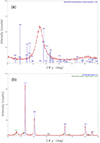 |
Fig. 7 XRD profiles of the machined (a) electroless-plated NiP and (b) electroplated Cu surfaces. |
Peak fitting results of the obtained XRD profile of electroplated Cu surface.
The difference between the EBSD and XRD results arises from both their measurement principles and the nature of what they detect. EBSD identifies grains on the basis of orientation differences and merges slightly misoriented crystallites into a single grain if the misorientation is below the threshold angle. In contrast, XRD estimates the size of crystallites, i.e., coherently diffracting domains within a grain that correspond to subdomains of a crystal. Consequently, the crystallite sizes obtained by XRD analysis tend to be smaller, whereas the grain sizes measured by EBSD analysis appear larger. In any case, the electroplated Cu surface exhibits fine crystalline microstructures; thus, the sand-like texture observed on the machined electroplated Cu surface, as shown in Figure 2b, is considered to result from these fine microstructures. Moreover, a possible reason for the absence of the step structures on the machined electroplated Cu surface, as shown in Figure 1b, is that its crystal grains are too small to significantly affect the machining process.
4 Conclusions
We investigated the roughness and microstructures of the electroplated Cu machined by ultraprecision diamond turning, as well as those of the OFC and electroless-plated NiP for comparison.
The average RMS surface roughnesses measured over a large area of 140 μm × 105 μm using a WLI in ascending order were 0.83 nm for electroplated Cu, 1.26 nm for electroless-plated NiP, and 1.65 nm for OFC. Step structures were observed on the OFC surface, probably caused by crystal grains, leading to larger RMS roughnesses. Concentric waves were observed on the NiP plating; however, they are considered to be caused not by the material itself but by the motion error of the ultraprecision turning machine. The electroplated Cu surface appeared the smoothest with no step structures.
For a smaller area of 1 μm × 1 μm measured using an AFM, the average RMS surface roughnesses in ascending order were 1.44 nm for electroless-plated NiP, 1.74 nm for electroplated Cu, and 2.29 nm for OFC. The OFC surface showed tiny holes, whereas the electroplated Cu surface showed a sand-textured finish. In comparison, the electroless-plated NiP surface was smoother than the other two.
Focusing on the electroplated Cu, the results of PSD analysis can be summarized as follows. At spatial frequencies below 2 × 104 mm−1, the PSD of the electroplated Cu surface is lower than that of the OFC surface. When the range is narrowed to spatial frequencies below 1 × 103 mm−1, the PSD of the electroplated Cu surface becomes comparable to that of the electroless-plated NiP surface and remains lower than that of the OFC surface.
Microstructural analysis by EBSD revealed fine crystal grains on the electroplated Cu surface ranging from 40 to 280 nm, whereas XRD indicated smaller crystallite sizes of 20–47 nm, confirming that the electroplated Cu is fully crystallized and polycrystalline. The discrepancy between the EBSD and XRD results arises from differences in their measurement principles. In any case, the electroplated Cu was found to be composed of microcrystalline grains, as confirmed by both EBSD and XRD analyses. Therefore, the sand-like texture observed on the machined electroplated Cu surface is likely due to the presence of these microcrystalline grains. Moreover, a possible reason for the absence of the step structures on the machined electroplated Cu surface is that its crystal grains are too small to significantly affect the machining process.
Overall, the findings demonstrate that electroplated Cu provides superior surface smoothness and machinability compared with OFC, although it is slightly inferior to electroless-plated NiP at high spatial frequencies, highlighting its suitability for the ultraprecision machining of optical components, where both high shape accuracy and small surface roughness are essential.
Funding
This research received no external funding.
Conflicts of interest
The authors declare that they have no conflicts of interest.
Data availability statement
The data that support the findings of this study, including those not shown in this article, are available from the corresponding author upon reasonable request.
Author contribution statement
HT conceptualized and supervised the study, participated in all experiments, interpreted all the data, and wrote the manuscript. HA supervised and managed the machining experiments, and provided expert advice. MK supervised and managed the measurements, interpreted the data, and provided expert advice. All authors have read and approved the final manuscript.
Acknowledgments
We thank Hideyuki Aizawa of Sendai Nikon Corporation for turning the specimens. We also thank Hideki Munakata of Chiba Institute of Technology for measuring the surface topographies.
References
- Rhorer R, Evans C, Fabrication of optics by diamond turning, in Handbook of Optics, 3rd edn. Vol. II: Design, Fabrication and Testing, Sources and Detectors, Radiometry and Photometry, edited by Bass M, DeCusatis C, Enoch J, Lakshminarayanan V, Li G, Macdonald C, Mahajan V, Stryland EV, (McGraw-Hill, 2009), Chap. 10. [Google Scholar]
- Lucca DA, Klopfstein MJ, Riemer O, Ultra-precision machining: cutting with diamond tool, ASME. J. Manuf. Sci. Eng. 142, 11 (2020). https://doi.org/10.1115/1.4048194. [Google Scholar]
- Syn C, Saito T, Taylor J, Donaldson R, Materials properties influence on smoothness of diamond-turned electroless nickel, in Optical Fabrication and Testing Workshop, Technical Digest Series Optica Publishing Group, 1985), paper ThBB6. https://doi.org/10.1364/OFT.1985.ThBB6. [Google Scholar]
- Taylor JS, Syn CK, Saito TT, Donaldson RR, Surface finish measurements of diamond-turned electroless-nickel-plated mirrors, Opt. Eng. 25, 9 (1986). https://doi.org/10.1117/12.7973947. [Google Scholar]
- Syn CK, Taylor JS, Donaldson RR, Diamond tool wear vs. cutting distance on electroless nickel mirrors, in Proc. SPIE 0676, Ultraprecision Machining and Automated Fabrication of Optics, (1987). 10.1117/12.939527. [Google Scholar]
- Eda H, Kishi K, Ueno H, Masubuchi S, Ultra precision cutting of electroless nickel plating layer, J. Jpn. Soc. Precis. Eng. 53, 5 (1987). (in Japanese) https://doi.org/10.2493/jjspe.53.814. [Google Scholar]
- Eda H, Kishi K, Ueno H, Oyatsu M, For a long life of natural single crystal diamond tool—the investigation of ultra precision cutting for electroless Ni-P, J. Jpn. Soc. Precis. Eng. 55, 1 (1989). (in Japanese) https://doi.org/10.2493/jjspe.55.161. [Google Scholar]
- Pramanik A, Neo KS, Rahman M, Li XP, Sawa M, Maeda Y, Cutting performance of diamond tools during ultra-precision turning of electroless-nickel plated die materials, J. Mater. Process. Technol. 140, 1–3 (2003). https://doi.org/10.1016/S0924-0136(03)00751-9 [Google Scholar]
- Chon KS, Namba Y, Single-point diamond turning of electroless nickel for flat X-ray mirror, J Mech Sci Technol. 24, 8 (2010). https://doi.org/10.1007/s12206-010-0512-3. [Google Scholar]
- Pramanik A, Neo KS, Rahman M, Li, XP, Sawa M, Maeda Y, Ultra-precision turning of electroless-nickel: Effect of phosphorus contents, depth-of-cut and rake angle, J. Mater. Process. Technol. 208, 1–3 (2008). https://doi.org/10.1016/j.jmatprotec.2008.01.006. [Google Scholar]
- Yan J, Oowada T, Zhou T, Kuriyagawa T, Precision machining of microstructures on electroless-plated NiP surface for molding glass components, J. Mater. Process. Technol. 209 (2009). https://doi.org/10.1016/j.jmatprotec.2008.12.008. [Google Scholar]
- Brinksmeier E, Gläbe R, Schönemann L, Diamond micro chiseling of large-scale retroreflective arrays, Precis. Eng. 36, 4 (2012). https://doi.org/10.1016/j.precisioneng.2012.06.001. [Google Scholar]
- Chon KS, Takahashi H, Namba Y, Wear inspection of a single-crystal diamond tool used in electroless nickel turning, Opt. Eng. 53, 3 (2014). https://doi.org/10.1117/1.OE.53.3.034102. [Google Scholar]
- Milan N, Sorgato M, Parenti P, Annoni M, Lucchetta G, Effects of micromilled NiP mold surface topography on the optical characteristics of injection molded prismatic retroreflectors, Precis. Eng. 61 (2020). https://doi.org/10.1016/j.precisioneng.2019.10.006. [Google Scholar]
- Decker DL, Bennett JM, Soileau MJ, Porteus JO, Bennett HE, Surface and optical studies of diamond-turned and other metal mirrors, Opt. Eng. 17, 2 (1978). https://doi.org/10.1117/12.7972204 [Google Scholar]
- Moriwaki T, Okuda K, Machinability of copper in ultra-precision micro diamond cutting, Ann. CIRP, 38, 1 (1989). https://doi.org/10.1016/S0007-8506(07)62664-X. [Google Scholar]
- Sugano T, Takeuchi K, Yoshida Y, Diamond turning of oxygen-free copper for mirrors, JSME Int. J. Ser. C, 36, 4 (1993). https://doi.org/10.1299/jsmec1993.36.549. [Google Scholar]
- Zhang H, Zhang X, Factors affecting surface quality in diamond turning of oxygen-free high-conductance copper, Appl. Opt. 33, 10 (1994). https://doi.org/10.1364/AO.33.002039. [Google Scholar]
- Zhang X, Zhang Y, Study on the surface quality of a diamond-turned oxygen-free high-conductance copper reflector used in a high-power CO2 laser, Opt. Eng. 36, 3 (1997). https://doi.org/10.1117/1.601277. [Google Scholar]
- Tanaka H, Shimada S, Higuchi M, Yamaguchi T, Kaneeda T, Obata K, Mechanism of cutting edge chipping and its suppression in diamond turning of copper, Ann. CIRP, 54, 1 (2005). https://doi.org/10.1016/S0007-8506(07)60047-X. [Google Scholar]
- Ding X, Jarfors AEW, Lim GC, Shaw KC, Liu YC, Tang LJ, A study of the cutting performance of poly-crystalline oxygen free copper with single crystalline diamond micro-tools, Precis. Eng. 36, 1 (2012). https://doi.org/10.1016/j.precisioneng.2011.09.001. [Google Scholar]
- Mishra V, Biswas AK, Kumar N, Kukreja LM, Sarepaka RV, Fabrication of λ/2 phase step mirror for CO2 laser resonator using diamond turning, Opt. Eng. 53, 3 (2014). https://doi.org/10.1117/1.OE.53.3.036107. [Google Scholar]
- Takino H, Kawai T, Takeuchi Y, 5-axis ultraprecision machining of complex-shaped mirrors for extreme ultraviolet lithography system, Ann. CIRP, 56 1 (2007). https://doi.org/10.1016/j.cirp.2007.05.031. [Google Scholar]
- Takino H, Takeuchi Y, Machining of smooth optical surfaces by ultraprecision milling with compensated feeding mechanisms, Int. J. Autom. Technol. 13, 2 (2019). 10.20965/ijat.2019.p0185. [Google Scholar]
- Saito TT, Simmons LB, Performance characteristics of single point diamond machined metal mirrors for infrared laser applications, Appl. Opt. 13, 11 (1974). https://doi.org/10.1364/AO.13.002647. [Google Scholar]
- Waldrop F, Bezik M, Tewes W, Waldrop R, Electroplating application to the fabrication of optics, Appl. Opt. 14, 8 (1975). https://doi.org/10.1364/AO.14.001783. [Google Scholar]
- Sollid JE, Sladky RE, Reichelt WH, Singer S, Single-point diamond-turned copper mirrors: figure evaluation, Appl. Opt. 15, 7 (1976). https://doi.org/10.1364/AO.15.001656. [Google Scholar]
- Kimura WD, Saito TT, Glancing incidence measurements of diamond turned copper mirrors, Appl. Opt. 26, 4 (1987). https://doi.org/10.1364/AO.26.000723. [Google Scholar]
- Frost F, Takino H, Fechner R, Schindler A, Ohi N, Nomura K, Smoothing of diamond-turned copper surfaces using ion beams with aid of planarizing film, Jpn. J. Appl. Phys. 46, 9A (2007). https://doi.org/10.1143/JJAP.46.6071. [Google Scholar]
- Ebihara K, Yamamoto A, Kawai T, Takeuchi Y, Study on high efficiency machining with reaction-free shuttle unit, J. Jpn. Soc. Precis. Eng. 73, 2 (2007). (in Japanese) https://doi.org/10.2493/jjspe.73.220. [Google Scholar]
- Yoshikawa T, Kyoi M, Tanaka H, Onozuka H, Maeda Y, Taya M, Ultra precision cutting of roll die with micro lens array for plastic film, JSME Int. J. Ser. C, 77, 777 (2011). https://doi.org/10.1299/kikaic.77.2146. [Google Scholar]
- Mai QX, Daniels RD, Harpalani HB, Structural changes induced by heating in electroless nickel-phosphorus alloys, Thin Solid Films, 166, 1 (1988). https://doi.org/10.1016/0040-6090(88)90384-7. [Google Scholar]
- Bredael E, Blanpain B, Celis JP, Roos JR, On the amorphous and crystalline state of electrodeposited nickel-phosphorus coatings, J. Electrochem. Soc. 141, 1 (1994). https://doi.org/10.1149/1.2054703. [Google Scholar]
All Tables
All Figures
|
Fig. 1 Surface topographies measured with a WLI. |
| In the text | |
|
Fig. 2 Surface topographies measured with an AFM. |
| In the text | |
|
Fig. 3 Surface topography measured with an AFM: measurement result for a 10 μm × 10 μm area of the electroless-plated NiP cut surface. |
| In the text | |
|
Fig. 4 PSD curves calculated from topographies of various machined surfaces measured with a WLI. |
| In the text | |
|
Fig. 5 PSD curves calculated from topographies of various machined surfaces measured with an AFM. |
| In the text | |
|
Fig. 6 Results of EBSD analysis of the machined electroplated Cu surface. (a) Grain map and (b) grain size distribution histogram. |
| In the text | |
|
Fig. 7 XRD profiles of the machined (a) electroless-plated NiP and (b) electroplated Cu surfaces. |
| In the text | |
Current usage metrics show cumulative count of Article Views (full-text article views including HTML views, PDF and ePub downloads, according to the available data) and Abstracts Views on Vision4Press platform.
Data correspond to usage on the plateform after 2015. The current usage metrics is available 48-96 hours after online publication and is updated daily on week days.
Initial download of the metrics may take a while.