| Issue |
J. Eur. Opt. Society-Rapid Publ.
Volume 21, Number 1, 2025
EOSAM 2024
|
|
|---|---|---|
| Article Number | 24 | |
| Number of page(s) | 8 | |
| DOI | https://doi.org/10.1051/jeos/2025021 | |
| Published online | 26 May 2025 | |
Research Article
UV coatings using Ta2O5-SiO2 quantized nanolaminates
1
RhySearch, Institute for Optical Coatings and Characterization, Werdenbergstrasse 4, 9470 Buchs, Switzerland
2
Evatec Ltd, Hauptstrasse 1a, 9477 Trübbach, Switzerland
3
EMPA, Laboratory for Mechanics of Materials & Nanostructures, Feuerwerkerstrasse 39, 3602 Thun, Switzerland
* Corresponding author: manuel.baertschi@rhysearch.ch
Received:
31
January
2025
Accepted:
15
April
2025
The use of Quantized Nanolaminates (QNL) in optical interference coatings has gained significant attention in recent years. By using a magnetron sputtering tool from Evatec with rotating substrate table and multiple sputtering sources operating simultaneously, we are able to deposit these metamaterials consistently at exceptionally high rates, comparable to and sometimes even exceeding magnetron sputter rates for standard materials. This combination of high deposition rate and precision enables us to treat QNL as a stand-alone material, effectively replacing high-refractive index materials in complex interference filter designs. In our experiments, we used a combination of Ta2O5-SiO2 QNL to produce filters like anti-reflective and shortpass coatings within the UV range of 266–350 nm, which would be not possible with Ta2O5 as bulk material in similar designs.
Key words: Optical interference coatings / Quantized nanolaminates / Magnetron sputtering / Ta2O5 / SiO2
© The Author(s), published by EDP Sciences, 2025
 This is an Open Access article distributed under the terms of the Creative Commons Attribution License (https://creativecommons.org/licenses/by/4.0), which permits unrestricted use, distribution, and reproduction in any medium, provided the original work is properly cited.
1 Introduction
Quantized Nanolaminates (QNL) represent an innovative material system for optical coatings which was first developed by the Laser Zentrum Hannover (LZH) in 2016 [1]. This system involves the alternate deposition of two optical materials with different refractive indices as extremely thin layers, typically 0.1–2.0 nm thick. When numerous such layers are sequentially deposited on top of each other, they form a system which, as a stand-alone material has new optical properties compared to the standard bulk oxide materials. The refractive index of the resulting material is determined by the thickness ratio of the two constituent layers. However, the extreme thinness of the high index material layers in the stack, restricts the valence electron mobility, causing a shift in the absorption edge towards shorter wavelengths. This phenomenon has been demonstrated multiple times, primarily using Ion Beam Sputtering (IBS) or Atomic Layer Deposition (ALD) systems [1–3]. Unfortunately, the process of switching between the deposition of the two different coat materials, is time consuming, limiting the practical application of QNL in complex layer designs due to significant effort and costs. We have developed a magnetron sputtering process that allows the production of QNL systems from Ta2O5 and SiO2 as a continuous process [4]. This process achieves sputtering rates of up to 0.8 nm/s and enables the deposition of up to 2400 laminate pairs per hour without interruption during the process. For the first time, this advancement enables the economical use of QNL as an independent high refractive index material for complex optical filter systems. In this paper we demonstrate first our approach to develop QNL single layers. Subsequently, we use two different QNL variants as high refractive index materials to create two complex multilayer systems. The first is a shortpass filter below 320 nm with a reflective region after 340 nm. We compare it with a similar shortpass made with standard Ta2O5 layers as high refractive index material. Next, we present a double-side coated anti-reflective filter on quartz glass, which shows no significant absorption at 266 nm. This highlights the great potential of Ta2O5-SiO2 QNL compared to standard Ta2O5 based coatings when it comes to manufacturing filters for the UV range.
2 Material and methods
2.1 Quantized nanolaminates
At first glance the idea behind QNL appears to be a relatively simple system. They consist of the periodic and alternating stacking of materials with different band gap energies. The band gap energy describes the amount of energy that a photon must have to be absorbed by the valence electrons of the respective material. When a photon passes through these QNL, it experiences a periodic sequence of different potential energies, as shown in Figure 1.
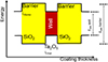 |
Figure 1 In this figure, the bandgap of the two different materials, building a QNL system are shown [5]. |
If the layer thickness of the “well” material is chosen to be sufficiently thin, an effect occurs where the bandgap of the entire system increases [1]. This can be understood as a restriction of the valence electron mobility within the material due to the thinness of the material layers, thereby making the absorption of light more difficult. The effective refractive index of the entire stack, on the other hand is only given by the volume ratio of the two materials and their own specific refractive indices [6].
This means, that by structuring mixed materials into ultra-thin layers instead of homogeneous mixtures, it is possible to obtain different bandgaps with the same refractive indices, since the band gap change depends only on the thickness of the well layers, but the refractive index depends on the mixing ratio, visualized in Figure 2.
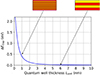 |
Figure 2 The graph shows the expected effect of QNL. Both systems shown schematically have the same mixing ratio of materials and consequently the same refractive index. However, the thinner layer structure increases the band gap of the left system. The figure has been modified from [2]. |
2.1 Experimental setup
The properties of QNL have already been demonstrated several times in different experiments and working groups, using different coating technologies. As each individual layer of the two different materials is extremely thin, a large number of them are required to produce a layer with a thickness in the range required for optical thin film designs. This leads to a problem for many standard manufacturing methods when it comes to producing QNL stacks economically and efficiently. One reason for this is that different processes are required for the different materials used, which have to be carried out alternately. Each of these must be set, stabilized, carried out and ramped down again before the next one can begin, which can greatly reduce the coating rate. Furthermore, it is hardly possible to monitor individual layers, as the sensitivity of both optical monitoring and the oscillating quartz method does not allow such high resolution to reliably measure layers below one nanometer. Due to possible drifts in processes, there is always a high risk that the thickness of the material layers cannot be kept constant in a stack of hundreds of them, which severely limits reproducibility. We benefit from a structural advantage provided by the Clusterline 200 BPM from Evatec, a magnetron sputtering system equipped with a rotating substrate table. To understand the benefits of this coating tool, it is necessary to first examine its working principles, as illustrated in Figure 3.
 |
Figure 3 Schematically drawn the tool with the sputter and plasma sources on top of it facing downwards on the table (left side). The opened tool with the rotating substrate table and the sources folded away (right side). |
The white wall separating the clean room from the gray room is visible at the front. Next to it is the control panel, positioned beside two automatic load locks, each capable of holding sixteen 8-inch substrates. Behind these load locks lies the vacuum transfer chamber, equipped with a handler, an aligner for precise substrate positioning, and a flipper. This flipper allows substrates to be turned for backside coating without breaking the vacuum. In the background, the large coating chamber can be seen. It houses a rotating substrate table with a capacity for sixteen 8-inch substrates, as shown in the picture on the right. The sputter sources are mounted on the chamber, with the system supporting up to four sources, each equipped with a different target material. The additional plasma source (PSC) in the background is capacitively coupled and operates with various gases, mainly for etching, increasing density, or oxidizing the sputtered layers. In our experiments to coat QNL, we use the two magnetron sputter sources at the front, fitted with a Si-target and a Ta-target. For producing pure SiO2 layers, we use the same Si-target in combination with the PSC source. To understand why our magnetron sputtering system is particularly well-suited for QNL production, it is helpful to first consider the standard process for creating single-layer materials. The system is designed for continuous table rotation during normal coating processes. Initially, the process gas is introduced, and the sputter source is activated with the shutter closed. Once the plasma stabilizes, the shutter opens, and the sputtering material is evenly deposited onto all substrates as the table rotates. Each rotation allows the layer to grow incrementally as the substrates pass under the source. The growth rate of this layer can be controlled either through calculations based on known rates or via optical monitoring, here the Evatec GSM1102 is used with both monochromatic and broadband monitoring algorithms. For QNL production, where two different materials are required, we operate two sources simultaneously. This setup necessitates stabilizing the system to prevent process drift. By doing so, we can deposit one layer of SiO2 and one of Ta2O5 with each table rotation, see Figure 4. The ratio between the two materials is adjusted by modifying the power supplied to the respective sputter sources. Additionally, the layer pair thickness can be fine-tuned by altering the rotation speed of the table; faster rotations yield thinner layers which amplifies the impact on the band gap. The ability to maintain a continuous process while depositing material from both sources simultaneously eliminates interruptions for alternating layers. This approach not only achieves a significantly higher deposition rate but also ensures a stable and consistent process. As a result, we can reliably produce uniform individual layers. This efficiency makes the production of QNL highly cost-effective, enabling its use as a standalone material in complex coating designs.
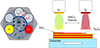 |
Figure 4 The diagram shows the process for producing QNL schematically. Due to the continuous process, a high rate and also a very stable behavior can be achieved. |
2.3 Material properties
We tested a variety of processes with different material ratios. All samples were coated for a duration of 900 s each, regardless of their deposition rate. For some selected combinations, we kept the process settings constant and only adjusted the table rotation speed, which is specified in seconds per rotation. This approach keeps the mixing ratio of the QNL within a set constant, but the thickness of the individual layers is altered. The lower the rotation time, the faster the table rotates, and the thinner the individual layers become. The transmission spectra of such a series are shown in Figure 5.
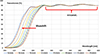 |
Figure 5 With the same source settings but different table rotation speed, a shift in absorption can be seen, while the refractive index and deposition rate stays constant. |
In the higher wavelength range, it can be observed that the measured spectra overlap, indicating that they must have the same refractive index as well as the same rate. In the lower wavelength range, the absorption edge shifts to shorter wavelengths for faster rotation speeds and correspondingly thinner individual layer thicknesses. Some of the layers were analyzed using HAADF STEM measurements. One of these layers is shown in Figure 6. This specific sample was coated with a table rotation speed of 6 s per pass for half an hour, resulting in 300 individual laminates and a total thickness of ~536 nm. Since we know the number of table rotations during the coating process and can determine via photospectrometry the thickness of the QNL stack, we are able to easily calculate the thickness of a single laminate pair. To calculate the thickness of each material within a laminate pair, we use the formula mentioned at the beginning. By knowing the refractive indices of the individual materials as well as from the overall block, it is possible to determine the volume fraction factor “f”, which allows us to calculate the average laminate thickness of both SiO2 and Ta2O5. The ability to analyze these layers using STEM HAADF image allowed us to additionally verify this formula. The average calculated thickness for SiO2 was found to be 1.35 nm, and for Ta2O5 it was 2.18 nm, while the STEM measurements showed an average thickness of SiO2 = 1.39 nm and Ta2O5 = 2.12 nm, respectively, which shows a high level of agreement. A line scan is shown in Figure 7.
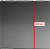 |
Figure 6 High-angle annular dark-field scanning transmission electron microscopy (STEM HAADF) image of a QNL cross-section which took 30 min of deposition time with rotating table at 6 s/pass. Measured at EMPA using a Titan Themis 200 G3. |
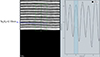 |
Figure 7 STEM HAADF image with a line scan for intensity shows a high level of agreement with the calculated thicknesses. |
From the transmission and reflection spectra, the band gap of the layers was calculated using a Tauc plot. By using the software OptiChar, the refractive indices, extinction coefficients and physical thickness can be determined across a wide wavelength range from the transmission and reflection spectra. From the total thickness and the measured refractive index, the individual layer thickness of the Ta2O5 laminates can be calculated using the presented formula for mixing refractive indices, since the number of table rotations during the 900 s coating time is known. The calculated band gaps are plotted against the Ta2O5 laminate thicknesses in Figure 8.
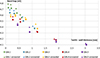 |
Figure 8 This figure shows the bandgap for the used sample sets compared to the thickness of the Ta2O5 laminates. Samples were measured directly after coating and after annealing. |
The different colors represent different process settings and thus different mixing ratios. Points of the same color correspond to different rotation speeds and, accordingly, different Ta2O5 thicknesses. All samples were annealed in ambient atmosphere at 450 °C for 1 h to reduce potential defects. The refractive indices of the samples are also plotted against the Ta2O5 laminate thickness in Figure 9.
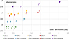 |
Figure 9 The refractive index at 550 nm compared to the thickness of the Ta2O5 laminates for the same samples as in Figure 8. Samples were measured directly after coating and after annealing. |
3 Results
As described in the previous section, the refractive indices and extinction coefficients were determined for all coated samples. This made it possible to select QNL settings with desired values for multilayer systems and create designs using OptiLayer, an optical interference design software. For the first filter, we chose a setting that provides a significant difference in the absorption edge compared to pure Ta2O5, while still maintaining a relatively high refractive index of n ≈ 1.8 (QNL5), to design a short pass filter. We built a design with a transmission region in the UV range up to a transition range from 320 to 340 nm and a high reflection part from 340 to 380 nm. The transition edge was intentionally chosen to be close to the absorption edge of pure Ta2O5 to show the difference. The design was created in two variants: a classic one using Ta2O5 as the high refractive index material and SiO2 as the low-refractive-index material, consisting of a total of 40 layers. The same analogue design with 40 layers was also created using the selected QNL setting to replace Ta2O5 as high refractive material, with slight adjustments. This design consists of 20 layers of SiO2 and 20 layers of QNLs, arranged alternately. Each QNL layer consists of a multiple of laminate pairs made of Ta2O5 and SiO2. The thickness of the individual SiO2 and Ta2O5 laminates was calculated as SiO2 = 1.36 nm and Ta2O5 = 1.00 nm, resulting in a pair thickness of 2.36 nm. Each of the 20 QNL blocks in this optimized design has its own thickness, ranging from 47 nm to 60 nm, which results in a total QNL thickness of 1016 nm and thus approximately 430 laminate pairs within the design. These two designs were then coated using optical monitoring and subsequently measured with a spectrophotometer.
In Figure 10, the shortpass filter using QNL as the high-refractive-index material is shown in blue, while the one with Ta2O5 is shown in red. The transmission spectra are illustrated with solid lines for both, and it can be seen that the design with QNL allows for a larger transparent range in the UV region until absorption (dotted line) prevents further use. This curve clearly shows that the chosen mixture is usable for an additional 20 nm into the shorter wavelength range. However, in the dashed reflection spectra, it is also evident that due to the lower refractive index, the width of the mirror region is significantly narrower compared to the Ta2O5 based design.
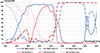 |
Figure 10 The shortpass with QNL (blue) and the shortpass with Ta2O5 (red). The solid line shows the transmission, the dashed the reflection and the dotted the loss. Both designs have a total of 40 layers. |
As another experiment, a QNL mixture with a very low refractive index of n ≈ 1.6 (QNL1) was chosen. This allowed for the creation of a very deep absorption edge. Using this, it became possible to design an antireflection coating with 6 layers at 266 nm. A quartz glass was coated on both sides with the design and measured using a photo spectrometer, as shown in Figure 11.
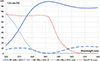 |
Figure 11 A double-side anti-reflective coating. The blue solid line indicates the transmission, the dashed the reflection and the dotted the absorption spectrum. The dotted red line shows the absorption spectrum of a Ta2O5 single layer. |
The spectrum is shown in blue, with the solid line once again representing the transmission in this case. It can be seen that it reaches a value of over 99% at 266 nm. The dashed line represents the reflection, which is 0.2% at 266 nm, and the dotted line represents the absorption. Based on the red dashed line, which shows the absorption of Ta2O5, it can be observed that this antireflection coating is practically free of absorption at 266 nm, whereas Ta2O5 would already absorb 70% of the incoming light at this wavelength, making it unusable for this application.
4 Discussion
In this work, we were able to demonstrate that we are capable of producing QNL with high rates and very stable properties using the Clusterline 200 BPM coating tool from Evatec through a process we developed. We subsequently coated, measured, and evaluated a variety of these QNLs with different refractive indices and band gaps. TEM measurements allowed us to confirm the structure. We then used two different QNLs to coat two designs that we considered suitable. In both processes the layers were terminated using optical broadband monitoring. The first design represents a short pass system consisting of 40 layers. Since we also produced a comparable design using Ta2O5, we were able to compare the two spectra. It is evident that, due to the lower absorption edge of the QNL, a larger transmission range exceeding 90% is achieved compared to the Ta2O5 design. The absorption of Ta2O5 typically starts to grow significantly at the edge around 310 nm. With the chosen QNL mixture, this edge was successfully shifted by 20 nm into the shorter wavelength range. However, it can also be observed that, due to the mixing behavior of the QNL and the resulting lower refractive of n = 1.8 instead of n = 2.1, the width of the high reflection region is narrower. The second design describes an antireflection coating that was coated on both sides of a quartz glass. For this design, which consists of a total of 6 layers on each side, a QNL setting with a refractive index of n = 1.6 was used. This also shifted the absorption edge by about 60 nm, resulting in a significantly larger usable range. This allows us to significantly expand the application range of Ta2O5 by structuring it with SiO2 as laminates into a range that would normally not be achievable with Ta2O5 as bulk material in a system at all.
Funding
This work is funded by Innosuisse, the Swiss agency for innovation promotion in the project 110.023 IP-ENG “QUINTESSENCE – Quantized nanolaminates as industrial magnetron sputtering process”.
Conflicts of interest
There is no conflict of interests.
Data availability statement
Data underlying the results presented in this paper are not publicly available at this time but may be obtained from the authors upon reasonable request.
Author contribution statement
Conceptualization: Manuel Bärtschi, Stephan Waldner, Silvia Schwyn Thöny, Xavier Maeder, Vivek Devulapalli, Fabian Steger, Thomas Frei.
Optical designs: Manuel Bärtschi.
Process development: Manuel Bärtschi, Fabian Steger.
Monitoring strategy: Stephan Waldner, Thomas Frei, Manuel Bärtschi.
Measurements: Manuel Bärtschi, Xavier Maeder, Vivek Devulapalli, Fabian Steger.
Software: Thomas Frei, Manuel Bärtschi.
Analysis: Manuel Bärtschi.
Visualization: Manuel Bärtschi, Silvia Schwyn Thöny.
Writing: Manuel Bärtschi.
Review: Stephan Waldner, Silvia Schwyn Thöny, Xavier Maeder.
References
- Willemsen T, Geerke P, Jupé M, Gallais L, Ristau D, in Proceedings of SPIE Laser Damage Conference, Boulder, edited by G.J. Exarhos, V.E. Gruzdev, J.A. Menapace, D Ristau, M.J. Soileau (SPIE, Bellingham, 2016), p. 10014. https://doi.org/10.1117/12.2244828. [Google Scholar]
- Steinecke M, Badorreck H, Jupé M, Willemsen T, Hao L, Jensen L, Ristau D, Quantizing nanolaminates as versatile materials for optical interference coatings, Appl. Opt. 59, 236 (2020). https://doi.org/10.1364/AO.379131. [Google Scholar]
- Jupé M, Willemsen T, Liu H, Steinecke M, Jensen L, Ristau D, Manufacturing of Quantized Nanolaminates (paper TB.4) (Optica Publishing Group, 2019). https://doi.org/10.1364/OIC.2019.TB.4. [Google Scholar]
- Schwyn Thoeny S, Baertschi M, Baselgia M, Batzer M, Process to deposit quantized nano layers by magnetron sputtering, WO2024/056313A1 (Patent) (World Intellectual Property Organization: International Application Published under the Patent Cooperation Treaty, 2024). [Google Scholar]
- Schwyn Thoeny S, Baertschi M, Batzer M, Baselgia M, Waldner S, Steinecke M, Badorreck H, Wienke A, Jupé M, Magnetron sputter deposition of Ta2O5-SiO2 quantized nanolaminates, Opt. Express 31, 15825 (2023). https://doi.org/10.1364/OE.487892. [Google Scholar]
- Feldman A, in Proceedings Modeling of Optical Thin Films, San Diego (1988), p. 0821. https://doi.org/10.1117/12.941850. [Google Scholar]
All Figures
|
Figure 1 In this figure, the bandgap of the two different materials, building a QNL system are shown [5]. |
| In the text | |
|
Figure 2 The graph shows the expected effect of QNL. Both systems shown schematically have the same mixing ratio of materials and consequently the same refractive index. However, the thinner layer structure increases the band gap of the left system. The figure has been modified from [2]. |
| In the text | |
|
Figure 3 Schematically drawn the tool with the sputter and plasma sources on top of it facing downwards on the table (left side). The opened tool with the rotating substrate table and the sources folded away (right side). |
| In the text | |
|
Figure 4 The diagram shows the process for producing QNL schematically. Due to the continuous process, a high rate and also a very stable behavior can be achieved. |
| In the text | |
|
Figure 5 With the same source settings but different table rotation speed, a shift in absorption can be seen, while the refractive index and deposition rate stays constant. |
| In the text | |
|
Figure 6 High-angle annular dark-field scanning transmission electron microscopy (STEM HAADF) image of a QNL cross-section which took 30 min of deposition time with rotating table at 6 s/pass. Measured at EMPA using a Titan Themis 200 G3. |
| In the text | |
|
Figure 7 STEM HAADF image with a line scan for intensity shows a high level of agreement with the calculated thicknesses. |
| In the text | |
|
Figure 8 This figure shows the bandgap for the used sample sets compared to the thickness of the Ta2O5 laminates. Samples were measured directly after coating and after annealing. |
| In the text | |
|
Figure 9 The refractive index at 550 nm compared to the thickness of the Ta2O5 laminates for the same samples as in Figure 8. Samples were measured directly after coating and after annealing. |
| In the text | |
|
Figure 10 The shortpass with QNL (blue) and the shortpass with Ta2O5 (red). The solid line shows the transmission, the dashed the reflection and the dotted the loss. Both designs have a total of 40 layers. |
| In the text | |
|
Figure 11 A double-side anti-reflective coating. The blue solid line indicates the transmission, the dashed the reflection and the dotted the absorption spectrum. The dotted red line shows the absorption spectrum of a Ta2O5 single layer. |
| In the text | |
Current usage metrics show cumulative count of Article Views (full-text article views including HTML views, PDF and ePub downloads, according to the available data) and Abstracts Views on Vision4Press platform.
Data correspond to usage on the plateform after 2015. The current usage metrics is available 48-96 hours after online publication and is updated daily on week days.
Initial download of the metrics may take a while.